This file type includes high-resolution graphics and schematics when applicable.
Verifying analog and mixed-signal circuits in Microsoft’s graphics chips presents challenges not addressed by RTL verification approaches. Analog and digital block interfaces are especially challenging, since accurate SPICE netlists aren’t available until much later in the design cycle. This delay in availability creates a major bottleneck in the design cycle, as the digital control logic has input dependencies coming from the analog portion of the design. Specifically, digital functional verification is compromised unless accurate analog signals are available.
Previous flows consisted of using “SystemVerilog only” models to represent analog circuits in the initial phase of the design cycle. But increasing complexity and the high number of interactions between the analog and digital portions of the design expose many regions of functional coverage that can be hit only in mixed-signal mode. Even when an analog-circuit netlist is available, lengthy simulation run times create a slowdown, which often results in only a small subset of tests within a regression being run in mixed-signal mode during the design’s pre-silicon verification stage.
As designs shrink to 18-nm and smaller geometries and grow in complexity, the above-mentioned limitations have an exponentially larger impact on design schedules and silicon time-to-market. The bottom line is that neither flow—the highly accurate “SystemVerilog+SPICE” flow nor the less accurate “SystemVerilog only” flow—can meet the needs of comprehensive silicon verification. What’s required is a middle ground in which full functional verification of digital logic can be accomplished without compromising the scope and accuracy of analog-circuit representation.
The solution, created collaboratively by Microsoft and Synopsys, is to build representations of complex analog circuits through granular models written using SystemVerilog “real” constructs.1 Although these models are at a slightly higher level of abstraction than the equivalent SPICE netlist, their accuracy is sufficient for the simulations to be considered “mixed-signal.” This claim of sufficient accuracy can be quantified via a static and fully automated flow that takes two waveform dumps, one of the SPICE simulation and the other of simulation of real number modeling (RNM)-based models, as input and makes a comparison of individual signals.
Target Design and Testbench
The full chip is for a graphics application. However, due to space limitations, the following in-depth description is that of the AMS subsystem only.
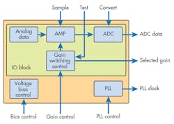
As shown in Figure 1, this design includes two main blocks:
1. Phase-locked loop (PLL): This block generates a PLL block for digital, based on PLL controls.
2. IO block: This block converts analog data (i.e., voltage) into digital data using an amplifier (AMP) and analog-to-digital converter (ADC). Based on the input analog voltage, the IO block selects the optimum gain to represent digital data.
Gain switching control is responsible for selecting optimum gain based on input analog data. The process to convert data from analog to digital happens via three individual input control signals: Sample, Test and Convert. These three steps are asserted one by one to perform the operation:
1. Sample: The AMP reads input and generates output based on selected gain.
2. Test: The gain-control logic checks whether or not it should lower amp gain. If gain control changes gain, AMP needs to regenerate output based on changed gain.
3. Convert: The ADC reads input and converts the input value into digital code.
RNM Coding
Below is some sample code from the design described in Figure 1. Both of the blocks described below don’t comprise the complete schematic of the circuits; they’re a higher abstraction, which gives information on the input and output signals and the mathematical representation of the algorithm. These simply provide ideas for coding models using a SystemVerilog “real” construct.
AMP circuit
Below is associated code for the AMP model. The gating trigger for the amplifier is the “bias” signal of VDD and VSS. The factor of amplification between input and output can be mathematically represented by:
Factor of Amplification = 0.8 + (diff/2), whereâ¦.
diff = (input1-input2) * (gain*0.4)
The “real” variables in this code are the inputs and outputs:
module amp (inp, inn, outp, outn, gain, VDD, VSS);
  input inp;
  input inn;
  output outp;
  output outn;
  input gain;
  input VDD;
  input VSS;

  real inp;
  real inn;
  real outp;
  real outn;
  logic [3:0] gain;
  wire VDD;
  wire VSS;

  real diff;

  logic power_ground_bias_ok = 0;
  always @(VDD or VSS)
  power_ground_bias_ok = VDD & ~VSS;

  always @* begin
    if (power_ground_bias_ok) begin
  diff = (inp - inn) * (gain * 0.4);

   outp = 0.8 + diff/2.0;
  outn = 0.8 - diff/2.0;
    end
  end

endmodule : amp
ADC Circuit
Below is the code for the ADC model. The gating trigger for the ADC is the same as for the AMP block, and is the “bias” signal of VDD and VSS. The output is generated synchronous to the “conv” signal. The algorithm to calculate the output of the ADC can be captured in the following equations, which are synchronous to VSS or VDD:
Output = Next lowest positive number of
{512 + (input1-input2)/(1/1023)} without exceeding 1023
module adc (inp, inn, out, conv, VDD, VSS);
  input inp;
  input inn;
  output out;
  input conv;
  input VDD;
  input VSS;

  real inp;
  real inn;
  logic [9:0] out;
  wire VDD;
  wire VSS;
  wire conv;

  int val;

  logic power_ground_bias_ok = 0;
  assign out = val;

  always @(VDD or VSS)
    power_ground_bias_ok = VDD & ~VSS;
  //update output when conv changes
  always @(power_ground_bias_ok or posedge conv) begin
    if (power_ground_bias_ok) begin
  val = $floor((inp-inn) / (1.0/1023));
  val = 512 + val;

   if (val < 0) val = 0;
  if (val > 1023) val = 1023;
    end
  end
endmodule : adc
Equivalence Checking
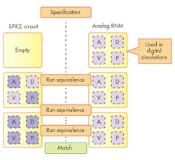
Equivalence checking is done to validate the accuracy of the RNM models based on the premise that two different representations of the same analog circuit, when given the exact same input stimulus, will have matching output. As Figure 2 shows, in this approach, one implementation is the SPICE netlist and the second implementation is the RNM-based SystemVerilog model. Both use the same original design specification as the basis for development.
In the initial phase of the design cycle, the simulations and testing use input stimuli that are unique to their flows. However, the recommended approach is to measure the model’s accuracy based on a “real” construct with that of the actual circuit. Thus, a common input stimulus is used only after both implementations achieve an acceptable level of code stability and maturity.
Once the common input stimulus has been created, the respective simulation environment (i.e., SPICE or SystemVerilog) is reused to generate a separate waveform dump file (in fsdb format). These files form the basis of the equivalence checking, generating a report that can be visualized.
Extracting Input Vectors
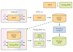
The three steps that comprise the input vector extractions (Fig. 3) are independent of which design representation is available first. This flexibility was an important consideration in architecting the solution to ensure that both analog and digital design can progress in parallel. The goal was to ensure equivalence of input vectors during simulations of both representations. The steps are:
1. An output simulation waveform dump file (in fsdb format) is created for either the SPICE netlist or the behavioral model (whichever is available earlier in the design cycle).
2. The input stimulus vectors are extracted from the fsdb file.
3. These input vectors are re-run on the design representation that’s available later in the design cycle. This guarantees that both the representations will have the same input stimulus.
Equivalence Compare and Simulation Run
Once the input vectors are available from the first design representation, they’re “replayed” on the second. It’s important to note that the second representation doesn’t have a testbench to drive any input stimulus or do any self-checking of outputs from a simulation. The output of the circuit is simply in response to stimulus and is captured for analysis. After this replay, a waveform dump (i.e., fsdb file) is available for both the SPICE netlist and the RNM-based model. These two fsdb files serve as the basis for equivalence checking (Fig. 3, again).
The key metrics for the values measured for each signal within the circuit are:
• Time range for the comparison
• Value tolerance during the compare
• Sample time of the compare
Equivalence Checking of Results and Output Analysis
Prior to equivalence checking, the individual signals need to be mapped, along with their acceptable tolerance values. This mapping needs to be done twice, and can be referred to as “input mapping,” which is used during the “replay” phase of the simulation, and “output mapping,” which is used for the “compare” portion of the flow. Below is a mapping representation of an inverter circuit:
where the yellow highlight is for the SystemVerilog signal, and the red is the SPICE representation (for both output and input mapping).
One additional argument needed in the output phase is the “tolerance,” shown in green:
As mentioned, tolerance implies the range in which the signal compare is still considered valid or passing. Specifically, the compare is a fail only if the difference between the two simulations exceeds the tolerance.
The equivalence-checking results are available in two basic flows: waveform compare in an fsdb viewer; or signal-compare output in a log file. The difference between these two flows is that option 1 is visual (manual) and option 2 is automated. Option 2—automated signal-compare—is described below.
Signal Compare Output in a Log File
This option required Synopsys to develop a VC Apps application for comparing a SPICE-based fsdb file with an fsdb file from an RNM code simulation. The important arguments for the application, called npi_analog_fsdb_cmp, are:
• Both the fsdb files.
• Mapping information for the individual signals.
• Tolerance level for acceptable comparison (recommended: within 10% accuracy of each signal).
• Selection of metrics important to the user (recommended: include all signals in the circuit data path and any signals associated with accurate behavior of the circuit).
A sample command is:
%> npi_analog_fsdb_cmp -output cmp.rpt -fsdb1 ana1.fsdb -fsdb2 ana2.fsdb -map cmp.map -time_unit ps -time_range 0 190000 -cycle 200 -shift 5 -max_error 10Conclusions
The collaboration between Microsoft and Synopsys yielded RNM-based analog models whose simulation speeds were measured to be 20X faster than equivalent circuits in SPICE. This allowed Microsoft to increase the number of tests that can be run in mixed-signal mode simulations. The simulation speeds RNM models. Also, there was a significant increase in the accuracy of Microsoft’s analog models, validated by equivalence checking.
Although accuracy of the models is comparable to the SPICE netlist with respect to representation of the continuous signals, note that these models don’t provide manufacturing process dependencies, temperature information, or parasitics. The RNM-based code should be considered an aid to behavioral modeling, and not a standalone, fully accurate simulation of the circuit.
That said, the success of these efforts yielded a long-term plan to integrate these tests into full-regression runs and potentially add them to the “design release” qualification test suite used by Microsoft to qualify design changes for future release of derivative products.
Reference:


