This file type includes high resolution graphics and schematics when applicable.
In high-performance semiconductors, the back-end-of-line (BEOL) interconnect pitch has been shrinking for decades following Moore’s law. Steady advances in very-large-scale integration (VLSI) technology for both digital and analog devices could never have been achieved without overcoming various reliability risks in IC chips as well as packages.
In many cases, such challenges do not reside solely in a package or an IC chip. Rather, the interaction between them is important. For example, the coefficients of thermal expansion (CTEs) of the silicon die and package materials, such as plastic molding compounds or organic substrates, differ significantly. This CTE mismatch induces thermo-mechanical stresses at the interfaces during thermal excursions, which can compromise the chip’s structural integrity. The influence of the package-induced stress on the chip is called chip-package interaction (CPI), and it plays a key role in overall product reliability.
Examples of CPI Problems
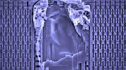
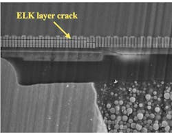
To meet electrical performance requirements of high-performance CMOS devices, engineers use low-k (dielectric constant), and more recently ultra-low-k (ULK) or extreme low-k (ELK), dielectric materials along with copper (Cu) interconnects. However, the mechanical strength of the material deteriorates with lower k, raising more concerns on thermomechanical reliability. The examples of the failure modes are inter-layer dielectric (ILD) cracking under bumps (Fig. 1), ILD delamination from die corners, and ILD fracture originating from die sawing defects.
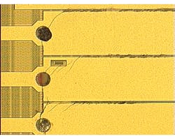
Increasing demands on power electronics often require wide and thick aluminum (Al) metallization plus an additional thick Cu layer to meet high-current and low-RDS(on) needs. Although the oxide dielectrics’ strength used in this technology is higher than that of the aforementioned low-k materials, the package shear stress can cause the Al metallization to plastically deform. This will eventually lead to passivation-overcoat (PO) layer cracking (Fig. 2) and/or metal extrusion. The risk becomes higher with increasing metal thickness and width.
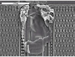
Recently, Cu wirebonding has been widely adopted due to its electrical performance and cost benefit compared to legacy gold (Au) wirebonding. Since Cu has a higher modulus and CTE than Au, it heightens the risk of ILD cracking (sometimes manifested as bond pad cratering, see Figure 3) and metal deformation under bond pads at assembly or during temperature-cycling reliability test.
How to Address CPI Risks
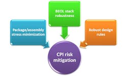
Three components control CPI risks (Fig. 4). First, package- or assembly-induced stresses on an IC chip play a critical role in CPI. The CTE mismatch between dissimilar materials in a package, e.g. Si chip, molding compound (MC), die attach compound, and leadframe, results in thermomechanical stresses during assembly processes and temperature cycling.
The package shear stress caused by MC is particularly important, because it directly contacts with the active side of the IC chip. CPI problems typically occur near chip corner and edge regions, where the shear stress reaches the maximum value. To reduce the shear stress, package materials have to be down-selected based on the mechanical properties and their thermomechanical influences on package stresses.
Another example is the underfill material selection in flip-chip ball-grid-array (FC-BGA) packages. If an underfill has a high elastic modulus or high glass transition temperature (Tg), it can cause ILD (especially low-k) damage due to thermomechanical stresses. In contrast, an underfill with low Tg can lead to solder-bump cracking.2
In addition to the materials selection, assembly process optimization is another important consideration for reducing CPI risks. Cu wirebonding has received lots of attention since its recent adoption, because a higher bonding energy transfers to the BEOL stack compared to Au wirebonding. Gross damage can be easily screened out during an early development cycle or by the final test. However, marginal damage that escapes from the final test may fail during temperature-cycling test when thermomechanical stresses exacerbate the damage. Thus, thorough wirebonding optimization has to be performed, including process corner studies and reliability assessment.
The second component in controlling CPI risk involves enhancing the BEOL stack robustness, which increases the strength for withstanding package- or assembly-induced stresses. Plastic deformation of the Al metal interconnects occurs when the package shear stress exceeds the yield stress of the metal. As this irreversible damage accumulates with the temperature-cycling stress, the metal layer loses its capability to resist the stress and “flows.”3 This eventually leads to the BEOL interconnect failure, such as passivation or ILD cracking and/or metal extrusion. Thus, it’s better to have a higher yield stress of the metal layer.
Although it’s known that a thicker Al film has a lower yield stress,4 a thicker metal layer is often needed to enable a higher current-carrying capability. The associated higher risk can be mitigated in multiple ways. Al and barrier metal deposition processes, as well as thermal treatment, can be further developed and optimized to improve the microstructure, texture, and yield stress of the metal. Developing a mechanically more robust passivation layer, or thickening up such layer, also helps reduce the CPI risk. To further enhance the BEOL stack robustness, a stress buffer layer such as polyimide (PI) can be coated on the chip. It reduces the shear stress transferred from the MC to the BEOL stack.
The above two aspects are largely related to the material properties of package and BEOL materials. The third aspect of CPI is the metal layout design. The package shear stress due to a CTE mismatch increases exponentially with distance from the die center.5 Because a very high stress is expected at the die corners, a keep-out-zone (KOZ) is applied, where no circuitry is allowed.
Die-edge areas are also at relatively high risk. In this region, the metal layout design may need to follow certain design rules to ensure suppression of CPI failure modes. The stress that causes passivation cracking increases with the metal width.
Wide metal slotting is a common technique to reduce the effective metal width. If a wide metal structure is not properly slotted, it results in passivation cracking as shown in Figure 2. Metal slotting is also needed under bond pads. The compressive stress from wirebonding deforms underlying metal structures, which can lead to ILD cracking and metal extrusion. Slotting confines the metal between ILD “dams” and reduces the tendency of metal to flow under loading. On the other hand, these design rules may also limit the effectiveness of circuit design or, in some cases, even increase the die size. Therefore, it’s important to balance reliability and competitiveness.
A CPI test chip with appropriate test structures is considered a useful methodology to evaluate these essential components of CPI. For example, it can be used to select low-stress MC and evaluate the BEOL stack robustness. It’s particularly valuable when developing CPI design rules for new Si or interconnect technologies. Test structures with varying designs and dimensions are used to quantify potential risks based on empirical data and to make a competitive decision on design rules.
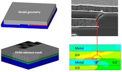
Since test-chip evaluation provides the extent of BEOL stack damage for a limited number of geometric variations and die locations, the empirical data can be further extrapolated using a simulation methodology. A crucial premise here is the correlation between the test-chip empirical data and modeling data. Once the correlation is established, the simulation methodology can be applied to a series of parametric models to develop comprehensive metal layout rules. Figure 5 illustrates an example of a finite-element-method (FEM) model that demonstrates a correlation between physical damage and simulation data.
Moving Forward
Clearly, CPI plays a critical role in achieving overall product reliability. Often, engineers will take advantage of CPI test chips to assess and address reliability risks. FEM modeling can be used to supplement the experimental test chip data and, once correlated, can help establish more comprehensive metal layout rules. The test-chip methodology allows proactive readiness for new metal stacks and interconnects.
Nonetheless, further developments are needed to improve overall cycle times and allow for rapid CPI assessment of Si, package, or layout iterations. Key challenges include improving Si and assembly process characterization to enhance the predictability of CPI responses and developing more advanced and efficient FEM simulation techniques. Overcoming these challenges will accelerate Si BEOL and assembly process optimization as well as make it more flexible, enabling higher-efficiency product-development cycles that meet reliability and cost needs.
This file type includes high resolution graphics and schematics when applicable.
Acknowledgement
The authors would like to thank Siva Gurrum and Hung-Yun Lin for their FEM modeling input.
References
1. Po-Jen Cheng, et al., “A Challenge of 45 nm Extreme Low-k Chip Using Cu Pillar Bumps as 1st Interconnection,” in Proc. 60th Electronic Components and Technology Conference (ECTC), May 2010, pp. 1618-1622.
2. K.M. Chen, et al., “Effects of Underfill Materials on the Reliability of Low-k Flip-Chip Packaging,” Microelectron. Reliab. 46, 155 (2006).
3. M. Huang, et al., “Plastic Ratcheting Induced Cracks in Thin Film Structures,” J. Mech. Phys. Solids, 50, 1079 (2002).
4. P. Alpern, et al., “On the Way to Zero Defect of Plastic-Encapsulated Electronic Power Devices—Part I: Metallization,” IEEE Trans. Dev. Mater. Reliab. 9, 269 (2009).
5. S. Groothuis, et al., “Computer Aided Stress Modeling for Optimizing Plastic Package Reliability,” in Proc. 23rd Ann. Reliability Physics Symposium, 1986, pp. 544-551.
Seung-Hyun Chae received his B.S. degree from Seoul National University, South Korea in 2003 and his Ph.D. degree from The University of Texas at Austin in 2010, both in materials science and engineering. His primary focus at Texas Instruments is IC-package reliability engineering. He has published more than 20 papers and two book chapters.
Amit Nangia currently manages the CPI and Reliability team in the Semiconductor Packaging organization of Texas Instruments. He holds a bachelor’s degree in metallurgical engineering from the University of Poona, India, and a master’s degree in materials science from the University of Texas at Arlington. His prior experience includes silicon-process technology development, wafer fab process engineering, and process integration, quality and reliability. He is a member of the Group Technical Staff, has authored and coauthored more than 10 papers, and holds one U.S. patent.
