Today’s complex system boards often contain application-specific processors, high-speed general-purpose processors, and multiple system-on-a-chip designs. Each of these high-performance circuits may have different clock-frequency requirements, since they weren’t necessarily designed to work with each other. Furthermore, each circuit on the board may have different timing constraints regarding the stability of the clock (jitter) and the clock period ratio (duty cycle).
This file type includes high resolution graphics and schematics when applicable.
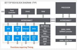
Thus, a key design challenge arises for these complex boards: Design a clocking subsystem that delivers multiple system clock signals and routes them to the chips to manage the timing of the many subsystems (Fig. 1). Such boards are typically designed for applications like set-top boxes/DVRs, high-end digital TVs, network switches and routers, data servers, and many other applications.
However, to keep the multiple clocks synchronized so that they can deliver maximum timing margins, there must be a low-jitter clock source that delivers multiple programmable clock outputs. Multiple, independent crystal oscillators on the board are no longer a reliable solution, because they can’t easily be synchronized. Furthermore, the cost of as many as five or six crystals and CMOS crystal oscillators for one board can add to the manufacturing cost, and they don’t provide spread-spectrum capability for EMI suppression.
Therefore, a highly integrated clock source with multiple phase-locked-loop controlled outputs offers the best solution to deliver the synchronized clock signals to the board’s various subsystems. Such a solution reduces board space and design complexity, and may lower system cost, too. Beyond that, the clock signals should be able to handle long routing paths on the circuit board without losing integrity. Long routes can pick up switching noise, cause signal deterioration due to capacitive loading, or encounter delays due to unusually long traces on the printed circuit board.
In a typical system such as a set-top box, the various subsystem blocks will operate at frequencies that are often based on the system function they must execute. Interfaces such as PCI or PCIe run at one frequency or a multiple of the base frequency depending on the required data-transfer rate. USB interfaces are similar, while Ethernet has multiple frequency requirements depending on the data rate. Additional functions such as a video signal, or main ASIC/processor, have their own clock requirements as well.
No matter the system application, jitter is a common concern for designers since it can negatively impact the timing margins on the multiple clock signals distributed on the circuit board. Moreover, as data rates and system clock speeds continue to climb, timing jitter has become a critical factor in system design. In many instances, the system performance limit is determined by system timing margin. Needless to say, a good understanding of the timing jitter becomes very important in system design.
Total jitter can be separated into random-jitter and deterministic-jitter components. Clock timing jitter can be measured in both the time and frequency domains. Period jitter, cycle-to-cycle jitter, and time-interval-error (TIE) jitter are measured in the time domain, while phase noise and phase jitter are measured in the frequency domain. Some sources of jitter include thermal noise, power-supply noise, crosstalk, and signal reflections.
Jitter Types
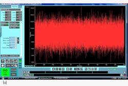
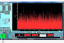
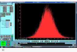
There are three forms of clock jitter, all of which can actually be present in a system. The scope traces in Figure 2, taken with the IDT 5P49V5901 clock-generator chip (a member of the company’s VersaClock 5 family), show the actual jitter types. They include:
• Period jitter: This form of jitter measures the maximum deviation of the clock period of a clock cycle in the waveform over a span of 10,000 clock cycles (Fig. 2a). The period-jitter RMS value measures the standard deviation of the clock period measurements over 10,000 clock cycles. The period jitter peak-to-peak value specifies the difference between minimum and maximum clock-period measurements over 10,000 clock cycles. The period jitter measurement is used to determine low-frequency jitter in applications by measuring the clock-period deviations over 10,000 clock cycles. Period jitter calculates the system timing margin. In Figure 2a, the period-jitter measurement shows an RMS measurement of 4.7 ps and a peak-to-peak measurement of 41.81 ps.
• Cycle-to-cycle jitter: This jitter type, specified as an RMS value, measures the change in clock period (standard deviation) between any two adjacent clock cycles over 1000 clock cycles. In addition, a peak-to-peak value of the cycle-to-cycle jitter measures the difference between minimum and maximum clock-period change between any two adjacent clock cycles over a span of 1000 clock cycles (Fig. 2b).The cycle-to-cycle jitter measurement is used to determine high-frequency jitter in applications and its value should be as small as possible to minimize its impact on system timing margins. Figure 2b shows an RMS cycle-to-cycle jitter measurement of 4.42 ps and a cycle-to-cycle jitter peak-to-peak measurement of 37.03 ps.
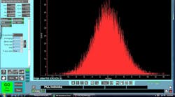
• Time-interval-error jitter: TIE jitter measures how far each active edge of the clock varies from the corresponding edge of an ideal clock (Fig. 2c). The TIE-jitter RMS value specifies the standard deviation of the timing error. The TIE peak-to-peak measurement defines the difference of the minimum and maximum timing error. TIE jitter is important in clock-and-data-recovery (CDR) PLLs to show if the PLL in the CDR is able to track to the incoming data stream. A large TIE-jitter value would show that the CDR PLL can’t properly track the variation in the incoming data stream. Figure 2c reveals an RMS TIE-jitter measurement of 3.29 ps, which results in a TIE-jitter peak-to-peak measurement of 27.93 ps.
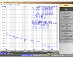
Phase noise also affects the quality of clock signals. It’s measured in the frequency domain, and calculated by taking the ratio of signal power to noise power, and normalizing it to a 1-Hz bandwidth at a given offset from the carrier signal. Phase jitter is measured by integrating the phase noise across specified frequency offsets from the carrier signal (Fig. 3). In this figure, the RMS phase-jitter measurement is 0.610 ps in the integration range of 12 kHz to 20 MHz.
Phase jitter measures the amount of energy present in the specified frequency offsets from the carrier signal, compared to the energy of the carrier signal by integrating the area under the phase-noise plot. For example, frequency is measured for SONET network interfaces by using a frequency offset of 12 kHz to 20 MHz from the carrier signal to integrate the area under the phase-noise plot. Similarly, Fiber Channel interfaces use a frequency offset of 637kHz to 10MHz from the carrier signal to integrate the area under the phase-noise plot.
System Implementation Options
When actually designing the system board that will contain the various chips, the decision process will likely follow these steps:
• Determine how many different clock frequencies are needed.
• Evaluate and determine the timing margins for the critical chips on the board.
• Check out available clock-generation solutions from various vendors and evaluate them for jitter, programmability, power consumption, and other factors needed for the solution.
• Lay out the circuit board with careful attention to the clock paths to prevent crosstalk and other factors that could affect the clock-signal quality.
• Program the clock chip to fine-tune it for the system application, adjusting output I/O levels, frequency, and other aspects.
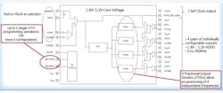
Multi-output clock generators have multiple sources. Therefore, deciding which to use will require some analysis of the chip features and matching those features to the intended application. As an example of the latest technical capabilities, the aforementioned IDT5P49V5901 programmable clock generator offers 0.7-ps RMS phase jitter, typical, and a core power consumption of less than 100 mW at 3.3 V (Fig. 4). With that low jitter value, clock chips can meet the PCIe Gen 1/2/3, USB 3.0, and 1/10 Gigabit Ethernet clocking requirements.
The VersaClock 5 series was designed for high-performance consumer, networking, industrial, computing, and data-communications applications, and can operate at input or output frequencies of up to 350 MHz. The chips offer four independent universal differential outputs capable of generating any output frequency. They’re also configurable as either LVPECL, LVDS, HCSL, or eight LV CMOS outputs. An on-chip one-time programmable (OTP) memory allows designers to store multiple configurations (clock frequency, I/O type, and other settings) for each of the four independent outputs.
Two select pins makes it possible to program up to four different configuration patterns, and have them be accessible using processor GPIOs or bootstrapping (one configuration pattern consists of programming data for all four clock output ports). The four configuration options may be used for different operating modes (full function, partial function, partial power-down), regional standards (U.S., Japan, Europe), or system production margin testing. The chip can also be configured to use one of its two I2C addresses, enabling multiple devices within a system.
This file type includes high resolution graphics and schematics when applicable.
A separate, on-chip I2C serial port also allows designers to load a new configuration into the configuration registers to either override the pre-stored settings or run through a test sequence. The frequencies on each of the outputs are generated from a single reference clock or crystal input. In addition, a glitchless manual switchover function makes it possible to select one of the redundant clock inputs during normal operation.
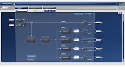
The multiple programmable features of chips like those in the VersaClock 5 series can be challenging to configure. To simplify the task, IDT’s Timing Commander software platform lets designers configure and program the VersaClock 5 chips using an intuitive and flexible graphical user interface (Fig. 5).
When designing complex system boards that contain multiple highly integrated chips, each with their unique clocking requirements, understanding the timing requirements for all becomes a challenge. Designers must deliver clock signals to each chip that meet the varied timing constraint, such as jitter and clock period ratio. By leveraging the latest generation of programmable clock generators that deliver multiple programmable outputs with very low jitter and flexible configuration options, designers can meet system timing demands for today’s designs and future-proof those systems when they go through upgrades.
