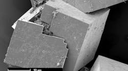
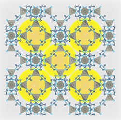
A research team from Belgium’s University of Leuven, the National University of Singapore, and Australia's CSIRO has adapted a production process normally reserved for semiconductors to create metal-organic frameworks (MOFs), a class of material that could lay the foundation for advanced microelectronics.
Metal-organic frameworks consist of a nanoporous grid of both organic molecules and metal ions. The material takes shape as the organic molecules push the metal ions apart, forming a regular pattern of small holes (or nanopores) that researchers have compared to a microscopic sponge. With all these pores, the material’s surface area ranges from 1,000 to 5,000 square meters per gram.
"The net result is a structure where almost every atom is exposed to empty space: one gram of MOF crystals has a surface area . . . the size of a football field,” says CSIRO researcher Mark Styles. "Crucially, we can use this vast space to trap other molecules, which can change the properties of a material.”
As reported in the journal Nature Materials, the researchers have uncovered a more efficient method for producing thin films of this material, which in the future could be grown directly on tiny electronic circuits. In laboratory experiments, the researchers demonstrated that the material could be made through chemical vapor deposition (CVD), a widely used manufacturing process for thin film semiconductors.
This revelation could represent a major step toward using the technology in microelectronics. “Vapor-phase deposition is already a common method to produce high-tech devices,” says Ivo Stassen, lead researcher from the KU Leuven Center for Surface Chemistry and Catalysis. As a result, new technologies using MOFs can be developed more quickly. Among these are sensors, nanochip components, and high-density batteries.
The massive surface area of the material could also help extinguish beliefs about the physical limits of semiconductor nodes. Manufacturers might be able to squeeze an unprecedented number of transistors into the material's huge surface area without taking up much space. MOFs have also shown potential as low-k dielectric semiconductor materials, which promise to reduce parasitic capacitance, boost switching speeds, and lower heat dissipation in tiny electronic devices.
Professor Rob Ameloot, the other lead researcher from the Center for Surface Chemistry and Catalysis, notes that the lack of a mainstream production process has largely confined MOFs to the laboratory. Until now, researchers have only been able to grow the material using a liquid solvent. Ameloot points out, however, that MOF crystals produced through this process are typically too large and impure for integrated electronics. In addition, using liquid solvents is not ideal for growing MOFs directly on electronic components.
In contrast, the Leuven research team was able to adapt a mass production process to the unique chemistry of MOF thin films. “We first deposit layers of zinc and let them react with the vapor of the organic material,” explains Stassen. “The organic material permeates the zinc, the volume of the whole expands, and it is fully converted into a material with a regular structure and nanopores.”
Stassen said that to refine the procedure, the researchers are collaborating with the Leuven-based semiconductor research center imec, which specializes in nanoelectronics. He notes that, along with imec, the university has submitted patents on the new process.
Imec has been investigating new ways to implant smaller and smaller transistors into computer processors and other electronics. The research center recently unveiled new advances that are laying the groundwork for silicon CMOS devices beyond the 5-nm node. However, the center also noted that it has begun investigating other approaches beyond silicon, such as spintronics and 2D materials, which could produce even smaller nodes.
Ultimately, the potential metal-organic frameworks is in its versatility. In December 2013, researchers from Sandia National Laboratory in New Mexico made one of the first major breakthroughs with the material, proving that they could create MOF thin films that conduct electricity. In a New York Times article, the researchers expressed hope that they would soon be able to customize the material's structure, coding electrical behaviors that are difficult to achieve with normal semiconductors.

