When it comes to power electronics, circuit designs usually are based on the performance and cost of the available semiconductor devices. Topologies are developed to take advantage of the capabilities of the active power devices and to mitigate their deficiencies. Active devices represent a significant fraction of the total system cost, so their number often is minimized.
Related Articles
- Lester Eastman: Compound Semiconductor Pioneer Leaves A Legacy Of Teaching
- GaN Roundtable: Learn The Truth About Gallium Nitride
- Master The Fundamentals Of Your Gallium-Nitride Power Resistors
As a result, single-switch circuit topologies such as the flyback are popular. Despite the well-documented performance disadvantages, half-bridge topologies often are used instead of full bridge as well. Relatively expensive magnetic and dielectric components are sometimes used to reduce the voltage stresses exerted on the semiconductor devices, allowing for reduced voltage ratings and thereby lower costs.
This file type includes high resolution graphics and schematics when applicable.
Complex control circuitry is used to implement resonant topologies to mitigate power losses induced by slow switching speeds. Significant volumes of capacitive and inductive elements are used to provide necessary quiescent output voltage levels while maintaining relatively low switching frequencies, again to avoid the consequences of the semiconductor devices’ poor switching speeds.
When significant advances in power semiconductor devices occur, subsequent radical changes are driven in circuit topology designs and their market adoption, such as the development of switched-mode power supplies after the introduction of commercially viable power MOSFETs. For example, the development of highly dense MOSFETs made the voltage regulator modules used to power modern processors viable.
The improved performance provided by super-junction MOSFET switches has enabled, at least in part, the rapid expansion in the use of power factor correction circuits. Similarly, the development of highly efficient insulated gate bipolar transistors (IGBTs) has largely enabled the use of energy-efficient inverterized motor systems.
The next wave of power electronics will use devices based on gallium nitride (GaN), specifically the GaN-AlGaN (aluminum gallium nitride) high electron mobility transistor (HEMT). These devices provide many benefits compared to silicon-based incumbents in a variety of power conversion applications such as class-D audio amplification and inverterized motion control, as well as ac-dc and dc-dc power supplies.
The Fundamentals
Efficiency, density, and cost can be directly related to the power device properties of conduction loss and switching loss. With MOSFETs, they’re called on resistance (RDS(on)) and switching charge (QSW). For an IGBT, they’re VCE(on) and (EOn+EOff), respectively. The lateral nature of the AlGaN-GaN HEMT provides for less terminal overlay capacitances and therefore less switching losses than the incumbent vertical silicon-based devices. In addition, the shorter drift regions in the HEMT, made possible by the larger bandgap (e.g., 3.3 eV) of GaN compared to silicon (e.g., 1.1 eV), together with the high electron mobility of the two-dimensional electron gas (2DEG), provide for lower specific on resistance. Therefore, the AlGaN-GaN HEMTs are inherently superior to silicon-based devices for power conversion applications.
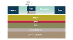
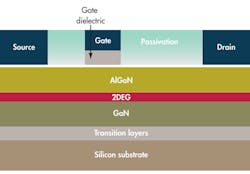
Basically, the GaN HEMT is a gated resistor (Fig. 1). The conduction path is formed near the interface between the GaN and AlGaN layers. Due to the polarizing nature of the AlGaN, net positive charges are effectively located at this interface. These charges produce a localized low-energy well in the bandgap edges. The highly polarizing nature of the AlGaN crystal further produces a built-in potential across the film.
When this potential exceeds a critical value (i.e. 1.5 to 2 V), atoms (presumably Al) near the surface of the film are ionized. The resulting free electrons are collected in the well of the band structure at the AlGaN-GaN interface. These electrons do not strongly interact with either the GaN or AlGaN lattices, forming a 2DEG, exhibiting high mobility (i.e., >2000 cm2/VS, compared to a silicon MOS inversion mobility of 1500 cm2/VS). In this way, 5 – 10 x 1012 electrons per cm2 can be incorporated in the 2DEG, providing a sheet resistivity of 300 to 500 Ω/sq.
The passivation of the AlGaN surface provides for the stability of the 2DEG. Ohmic contacts are made with the 2DEG through the passivating and surface AlGaN layers. Historically, this has been accomplished through an aluminum/titanium (Al/Ti) bi-layer capped with gold/titanium (Au/Ti) to promote mixing and prevent corrosion. But to make the devices cost-competitive with silicon-based alternatives, gold-free ohmic contact processes are required. Contact resistances of 0.2 to 0.5 Ω-mm then can be commonly achieved, with values as low as 0.05 Ω-mm reported. Reported devices have achieved linear source-drain resistances of 2 to 3 Ω-mm (30 V) and 10 to 20 Ω-mm (600 V).
Resistance is modulated through a field-effect inducing gate electrode. In the past, a metal-semiconductor (Schottky) gate was often used, especially for microwave amplifier applications. However, this structure is far too leaky (e.g., mA/mm of gate width) for use in power devices, where the typical device involved 100 to 3000 mm of gate width.
Therefore, state-of-the-art GaN HEMTs generally use insulated gate structures that exhibit far less leakage (e.g., pA/mm of gate width). To accommodate the large surface fields induced between the edge of the metallic gate electrode and the 2DEG, field plates must be engineered above the surface AlGaN layer. A highly effective fast switch then can be constructed for power conversion applications.
The Differences
Several important differences in behavior between such lateral AlGaN-GaN HEMTs and incumbent commonly used silicon-based power switches are key to their performance in application circuits.
One fundamental difference is the absence of a p-n junction in the GaN HEMT. In fact, spatially resolved p-n junctions in such GaN-based lateral HEMTs are technically impractical since AlGaN and GaN are unstable at temperatures above about 900°C, except in a growth environment. Even with a passivation layer of silicon nitride (SiN), the GaN or AlGaN material will disassociate at the surface, causing severe surface roughness, voids, and highly non-stoichiometric regions.
As the effective annealing of implantation damage, or the incorporation of dopants by implantation or diffusion, requires temperatures well in excess of 900°C, such strategies are ineffective in the formation of high performance p-n junctions. The absence of a p-n junction has at least two dramatic consequences for the behavior of AlGaN-GaN HEMTs.
First, no minority carriers are involved in the device’s operation. This is in stark contract to the behavior of MOSFETs, especially superjunction-based devices, as well as IGBTs. In both cases, the minority carriers that are injected into the drift region during the on state must be removed from the depletion region when the device is reverse biased, before current flow stops.
Significant energy loss results, as well as noisy ringing of the application circuit response during device switching, requiring sophisticated dead-time control and expensive filtering circuitry. In turn, this limits the applicability of superjunction MOSFETs, for instance, away from hard switching applications and sets a maximum operation frequency for both superjunction MOSFETs and IGBTs (e.g., less than 100 kHz).
The AlGaN-GaN HEMT does not suffer from these effects, so it switches much more cleanly with far less noise generation and the ability to operate at much higher frequencies (e.g., more than 1 MHz). This enables the reduction in filtering components, making the system smaller, lighter, and less expensive.
The reduced switching time reduces power losses. Also, the AlGaN-GaN system comprises wider-bandgap materials, so it’s intrinsically capable of higher temperatures. The HEMTs therefore have reduced cooling requirements, often eliminating the need for heatsinks. Or, they can operate with a higher ambient cooling medium (air or liquid).
The second major effect of the absence of a spatially resolved p-n junction is the lack of a switch-voltage diode clamp. In commonly used silicon-based power MOSFETs, a built-in diode clamps the source-drain voltage during, for instance, the back EMF-induced (electromotive force) voltage spike generated when switching current through an inductive element.
A p-n diode affords the possibility to non-destructively pass large currents, effectively clamping very large power sources. This is due to the phenomenon of multiplicative carrier generation (avalanche) across the energy gap between the upper valence and lower conduction band edges in the presence of a strong electric field. The relatively short distances present in the reverse biased p-n junction depletion region enables such a field.
This clamping diode has been very effectively used in power conversion applications, providing significant robustness for the use of silicon-based power devices. The limitation to this clamping mechanism occurs when the current through the semiconductor is sufficient to overcome the doping level and make a portion of the p-n junction intrinsic. At this point, a condition of thermal runaway from joule heating will destroy the device. This often is called the device’s avalanche capability. AlGaN-GaN HEMTs have no p-n clamping junction, so they have no avalanche capability.
Another significant difference is that commonly used (discrete) silicon-based devices collect the current vertically through a bulk drift region between the gate and drain, compared to the near surface drift region of the lateral HEMT. The silicon device then dissipates the Joule heating of the Ohmic conduction losses in a much (e.g., 100 times) larger volume of material. The local temperature rise, under short-circuit conditions, is far less in the vertical current collection case.
In addition, the vertical conduction case provides for the electric fields to be contained in the volume of the semiconductor material. This is not the case in the lateral HEMT, where the highest fields are present above the 2DEG, especially in the overlying dielectric layers, just beneath the gate/field plate conductors.
The absence of spatially resolved p-n junctions exacerbates the surface fields, since the conductive field plates induce much sharper discontinuities and therefore higher peak electric fields than can be achieved with the relatively smooth transitions provided by the presence of a semiconductor junction. The combination of these two differences means that the AlGaN-GaN HEMT is not characterized by the same tradeoff between drift length/doping (specific on resistance) and the avalanche breakdown critical field as commonly used silicon-based power devices.
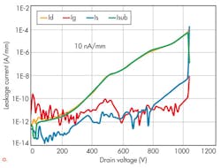
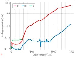
The equivalent design criteria for the lateral HEMT is the time-dependent dielectric breakdown of the insulating layers (including the AlGaN barrier) above the 2DEG. As such, reliable devices will operate below half of the breakdown field strength of these insulating layers. Therefore, there is significant headroom for voltage spikes between the rated operating voltage and the actual breakdown voltage of the HEMT device for a 600-V rated power HEMT from International Rectifier (Fig. 2). Typically, 5% to 10% of headroom is provided for silicon-based devices between the drain-source operating voltage rating and junction breakdown.
The AlGaN-GaN HEMT, therefore, represents a significant departure in terms of materials, device structure, and performance compared to incumbent silicon-based power devices.


