Optimizing Power Systems for the Signal Chain (Part 3)
This article is part of the Power Management Series: Optimizing Power Systems for the Signal Chain
Members can download this article in PDF format.
What you'll learn:
- How to optimize the ADRV9009 transceiver power system.
- PSMR and PSRR testing results.
- Testing results when using the LTM8063 µModule regulator (utilizing SSFM).
- Testing results for the optimized solution.
Part 1 of this signal-chain power-optimization series discusses how power-supply noise can be quantified to identify its effect on various parameters of signal-chain devices. An optimized power distribution network (PDN) can be created by determining the actual noise limits the signal-processing devices can accept without affecting the integrity of the signals they produce. In Part 2, this methodology is applied to high-speed analog-to-digital and digital-to-analog converters, where it demonstrates that lowering noise to a necessary level doesn’t always equate to higher cost, increased sized, and lower efficiency. These design parameters can actually be met in one optimized power solution.
This third and final part of the series focuses on another part of the signal chain—RF transceivers. Here, we check the sensitivity of the device to the noise coming from each power rail to identify those that need additional noise filtering. An optimized power solution is provided, which is further validated by comparing its spurious-free dynamic-range (SFDR) and phase-noise performance to the current PDN when attached to the RF transceiver.
Optimizing the Power System for the ADRV9009 Transceiver
The ADRV9009 is a highly integrated, radio-frequency (RF), agile transceiver with dual transmitters and receivers, integrated synthesizers, and digital-signal-processing (DSP) functions. The IC delivers the high performance and low power consumption demanded by 3G, 4G, and 5G macrocell time-division-duplex (TDD) base-station applications.
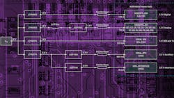
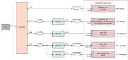
Figure 1 shows the standard PDN for the ADRV9009 dual transceiver. The PDN consists of an ADP5054 quad switcher with four linear regulators. The goal here is to see what performance parameters of the PDN can be improved, while producing noise that doesn’t degrade the performance of the transceiver.
As shown throughout this series,1, 2 quantifying the sensitivity of the ADRV9009 to power-supply noise is necessary to optimize the PDN. The ADRV9009 6-GHz dual RF transceiver requires five different power rails:
- 1.3-V analog (VDDA1P3_AN)
- 1.3-V digital (VDDD1P3_DIG)
- 1.8-V transmitter and BB (VDDA_1P8)
- 2.5-V interface (VDD_INTERFACE)
- 3.3-V auxiliary (VDDA_3P3)
Analysis
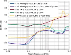
Figure 2 shows the Receiver 1 port PSMR results for the analog rails (VDDA1P3_AN, VDDA_1P8, and VDDA_3P3). For the digital rails—VDDD1P3_DIG and VDD_INTERFACE— the maximum injected ripple we could produce with a signal generator didn’t produce spurs in the output spectrum, so we don’t need to worry about minimizing ripple on those rails. Modulated spur amplitude is expressed in dBFS where the maximum output power (0 dBFS) is equivalent to 7 dBm or 1415.89 mV p-p in a 50-Ω system.
For the VDDA1P3_AN rail, the measurement was taken at two different branches of the transceiver board. Notice that in Figure 2, power-supply modulation ratio (PSMR) falls below 0 dB at <200-kHz ripple frequency, indicating that ripple at these frequencies produces even higher modulation spurs in the same magnitude. This means that below 200 kHz, Receiver 1 is very sensitive to even the smallest ripple produced by the VDDA1P3_AN rail.
The VDDA_1P8 rail is divided into two branches in the transceiver board: VDDA1P8_TX and VDDA1P8_BB. The VDDA1P8_TX rail reaches a minimum PSMR at 100 kHz at ~27 dB, corresponding to 63.25 mV p-p of 100-kHz ripple, resulting in modulated spurs of 2.77 mV p-p. VDDA1P8_BB measures a minimum of ~11 dB at a 5-MHz ripple frequency, equivalent to 0.038-mV p-p spurs produced by 0.136 mV p-p of injected ripple.
VDDA_3P3 data shows that at around 130 kHz and below, PSMR falls below 0 dB, indicating that the RF signal at Receiver 1 is very sensitive to noise coming from VDDA_3P3. The PSMR for this rail rises as the frequency increases, reaching up to 72.5 dB at 5 MHz.
In summary, the PSMR results show that among the power-supply rails, VDDA1P3_AN and VDDA_3P3 rail noise are the most worrisome, contributing the most significant ripple content coupled to Receiver 1 of the ADRV9009 transceiver.
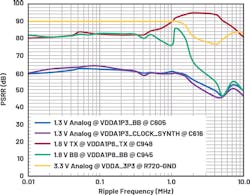
Figure 3 shows the power-supply rejection ratio (PSRR) performance of the ADRV9009 for the analog supply rails. VDDA1P3_AN’s PSRR is flat at ~60 dB up to 1 MHz, and it slightly falls to a minimum of ~46 dB at 5 MHz. This can be viewed as a 0.127 mV p-p of 5-MHz ripple that produces a 0.001 mV p-p spur riding the LO frequency together with the modulated RF signal.
The PSRR for the VDDA1P8_BB rail of the ADRV9009 bottoms out at ~47 dB at 5 MHz, while the VDDA1P8_TX rail’s PSRR doesn’t fall below ~80 dB. In the spectrum below 1 MHz, the PSRR of VDDA_3P3 is higher than the 90 dB that’s shown. The measurement is clipped at 90 dB as the maximum injected ripple up to 1 MHz is 20 mV p-p—not high enough to produce spurs above the noise floor of the local oscillator. The PSRR for that rail is higher than what’s shown below 1 MHz; as the frequency increases, it drops to 76.8 dB at 4 MHz, its lowest value in the 10-kHz to 10-MHz range.
Similar to the PSMR results, PSRR data shows that the majority of the noise coupled to the local oscillator frequency, particularly above 1 MHz, comes from the VDDA1P3_AN and VDDA_3P3 rails.
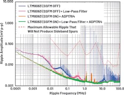
To determine if a power supply can meet noise requirements, the ripple output of the dc power supply is measured, resulting in a waveform plotted across a 100-Hz to 100-MHz frequency range, like that shown in Figure 4. An overlay is added to this spectrum—the threshold at which sideband spurs will appear at the modulated signal. The overlaid data is obtained by injecting sinusoidal ripple into the specified power-supply rail at several reference points, to see what ripple levels produce sideband spurs, as discussed in Part 1 of this series.
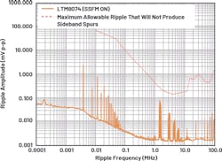
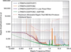
The threshold data shown in Figures 4 to 6 are for the three supply rails to which the transceiver is most sensitive. The power-rail spectra are shown for various dc-dc converter configurations, with and without spread spectrum frequency modulation (SSFM) enabled or additional filtering via an LDO regulator or low-pass (LC) filter. These waveforms are measured at the power-supply board to give room for additional margin that’s greater than or equal to 6 dB below the noise limit.
Testing
Figure 4 shows the spur threshold for the VDDA1P3_AN rail along with the measured noise spectrum for various configurations of an LTM8063 µModule regulator. As illustrated, using the LTM8063 directly powering the rail with SSFM disabled produces ripple at the LTM8063’s fundamental operating frequency and harmonics that exceed the threshold. In particular, the ripple exceeds the limit by 0.57 mV at 1.1 MHz, indicating that some combination of post-regulator and filter is needed to suppress the noise coming from the switching regulator.
If only an LC filter is added (no LDO regulator), the ripple at the switching frequency just reaches the maximum allowable ripple—there’s probably not enough design margin to ensure top performance of the transceiver. Adding an ADP1764 LDO post-regulator and turning on the LTM8063’s spread-spectrum mode lowers the fundamental switching ripple amplitude and its harmonics over the entire spectrum. In addition, the noise peaks due to SSFM in the 1/f region. The optimum result is achieved by turning on SSFM and adding both an LDO regulator and LC filter, which reduces the remaining noise caused by the switching action. This leaves an ~18-dB margin from the maximum allowable ripple.
SSFM spreads noise over a wider band, thereby reducing the peak and average noise at the switching frequency and its harmonics. This is done by modulating the switching frequency up and down by a 3-kHz triangle wave. This introduces new ripple at 3 kHz, which is taken care of by the LDO regulator.
When SSFM is enabled, the resulting low-frequency ripple and its harmonics are apparent in the VDDA_1P8 and VDDA_3P3 output spectrums shown in Figures 5 and 6, respectively. As can be seen in Figure 5, the noise spectrum of the LTM8074 with SSFM enabled provides a minimum ~8-dB margin to the maximum allowable ripple for the VDDA_1P8 rail. So, no post-regulator filtering is necessary to meet the noise requirements on this rail.
Figure 6 shows the noise spectrum for various configurations of the LTM8074 µModule regulator, along with the maximum noise requirements for the 3.3-V VDDA_3P3 rail. For this rail, we’re examining the results using the LTM8074 Silent Switcher µModule regulator. The LTM8074-only configuration (no filter or LDO post-regulator) produces noise that exceeds the limit regardless of whether spread-spectrum mode is enabled or disabled.
The results of two alternate configurations meet the noise specification with >6 dB margin: the LTM8074 without SSFM enabled plus an LC filter, and the LTM8074 with SSFM enabled with an LDO post-regulator. Although both meet the requirement with sufficient margin, the LDO post-regulator solution gets the edge here. This is because the VDDA_3P3 rail also provides the 3P3V_CLK1 clock supply. Therefore, a reduction of 1/f noise is relatively more important, as noise here could translate to phase jitter in the local oscillator if not addressed.
Optimized Solution
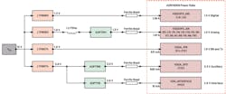
Based on the outcome of these tests, Figure 7 shows an optimized solution that would give >6-dB noise margin when used on an ADRV9009 transceiver board.
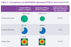
Table 1 shows the comparison of the optimized PDN to the standard PDN. The component area reduction is 29.8%, and the efficiency increased to 69.9% (from 65.7%) with an overall power saving of 0.6 W.
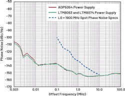
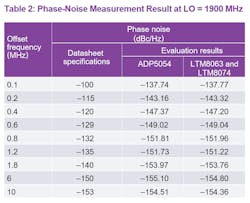
To validate the efficacy of this optimized power solution—in terms of systematic noise performance—a phase-noise measurement is performed. The optimized solution in Figure 7 is compared to the control case—an engineering release version of the ADRV9009 evaluation board—the AD9378 evaluation board using the PDN shown in Figure 1. The same board is used, but with the PDN depicted in Figure 7, and the phase-noise results were compared. Ideally, the optimized solution meets or exceeds the datasheet reference graphs.
Figure 8 shows the phase-noise results of the AD9378 evaluation board with the standard ADP5054-based power supply compared to the results from the same board using a power supply based on the LTM8063 and LTM8074. The µModule power solution has slightly better performance of around 2 dB vs. the ADP5054 power solution.
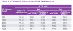
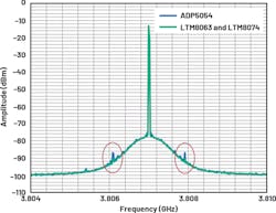
The transceiver’s SFDR measurement using both power solutions (Table 3) reveals comparable performance for both power solutions, except for LO = 3800 MHz where ADP5054’s switching ripple starts to produce modulation spurs on the carrier signal output spectrum (Fig. 9).
Conclusion
Different requirements for various applications could demand further improvement or changes in the power distribution networks of the evaluation boards. Being able to quantify the noise requirements of signal-processing ICs provides a more effective way of designing its power supply or even just optimizing the existing power solution.
For high-performance RF transceivers such as the ADRV9009, setting up noise injection in the PDN to identify how much power-supply noise is tolerable helped us make improvements in space requirements, efficiency, and, critically, thermal performance over the current PDN.
Read more from the Power Management Series: Optimizing Power Systems for the Signal Chain
References
1. Pablo Perez, Jr. and Patrick Errgy Pasaquian. “Optimizing Power Systems for the Signal Chain—Part 1: How Much Power Supply Noise Is Tolerable?” Analog Dialogue, Vol. 55, No. 1, March 2021.
2. John Martin Dela Cruz and Patrick Errgy Pasaquian. “Optimizing Power Systems for the Signal Chain—Part 2: High Speed Data Converters.” Analog Dialogue, Vol. 55, No. 2, April 2021.
Delos, Peter. “Power Supply Modulation Ratio Demystified: How Does PSMR Differfrom PSRR? ” Analog Devices Inc., December 2018.
Delos, Peter. “Transceiver Phase Noise Teardown Informs Performance Capability with an External LO.” Analog Devices Inc., October 2019.
Naeem, Naveed and Samantha Fontaine. “Characterizing the PSRR of Data Acquisition μModule Devices with Internal Bypass Capacitors.” Analog Dialogue, Vol. 54, No. 3, July 2020.
