Tips for Measuring Ultra-Low Bias Current with Commercial Lab Equipment
Members can download this article in PDF format.
This article is part of TechXchange: Why Low Iq is the Smart Thing to Do
What you'll learn:
- How to effectively measure ultra-low bias current by recreating the measurement scheme from an app note.
- Measuring input capacitance and input current.
- Creating a better measurement environment.
In applications that require low leakage current, it’s important to select a low-input-bias-current (IB) operational amplifier. The application note AN-1373 describes how to measure ultra-low bias current using the ADA4530-1 evaluation board. However, due to the nature of handling femtoampere-level currents, the measurement environment—equipment such as jigs, shields, cables, and connectors—also affect the measurement results.
This article will introduce a trial to recreate the measurement in AN-1373 using commonly available commercial-grade lab equipment, jigs, and materials, and includes some workarounds to improve the measurement to finally achieve 50 fA.
First, we measure the input capacitance for bias current and the variation of output voltage with charging of the input capacitance under the condition of 125°C. We also attempt to derive the bias-current value from the measured output voltage. Finally, we will try to improve the measurement environment based on the measurement results.
Capacitive Integration Measurement
According to AN-1373, the input capacitance (Cp) of the ADA4530-1 must be measured first in order to use the capacitance integral measurement method. We will perform this experiment using the ADA4530-1R-EBZ-BUF,with the ADA4530-1 configured in buffer mode.
Next, we calculate the input current (IB+). Specifically, using the circuit configuration shown in Figure 1, IB+ flows into the Cp when the SW in the test box is turned from ON (grounded to GND) to OFF (open). The output voltage rises as IB+ charges Cp, so that the value of IB+ can be calculated by monitoring and substituting it into Equation 1.
Measuring Total Input Capacitance with an Input Series Resistor
To calculate Cp, this experiment adopts a method using series resistance. Figure 2 shows a simple circuit diagram. The value of the series resistance is based on the measurement guidelines found on page 6 of AN-1373. The actual value is Rs = 8.68 MΩ. An SW also is mounted in the test box for later experiments (SW is open at this time).
The frequency at which the waveform from the function generator is attenuated to –3 dB can be measured; use Equation 2 to calculate the input capacitance.
Figure 3 shows the setup. Since the temperature in the temperature-controlled chamber rises to 125°C in the experiment described in the section “Measuring IB+ with Known Input Capacitance” (page 6 of AN-1373), we utilize materials that can withstand such a temperature. RG-316U was used as the material for the coaxial cable.
Furthermore, the noninverting inputs of the ADA4530-1 on the evaluation board are triaxial connectors. For this reason, a triax-to-coaxial conversion connector (BJ-TXP-1 from the Axis Company) was employed. In this configuration, the guard terminal on the triax side was left floating.
As a result of the measurement, Cp = 73.6 pF was obtained, which is a relatively large value since the actual measurement, according to AN-1373, is about 2 pF. The reason for this is related to the cable length from the test box—which looks more like a test board—to the noninverting input.
Measuring IB+ with Known Input Capacitance
Finally, we start to measure the bias current. The circuit configuration is shown in Figure 1, and Figure 4 illustrates the mounted test box. Note that the input resistor used in the section “Measuring Total Input Capacitive with an Input Series Resistor” is removed.
As described in AN-1373 (the capacitive integration measurement method, page 7), short-circuit the SW to GND, then open it and monitor the output voltage fluctuation with a digital multimeter (DMM) for a few minutes (we used the 34401A DMM from Keysight Technologies). Finally, calculate the IB+ by substituting VOUT into Equation 1.
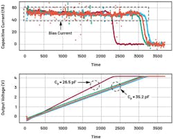
The results of three measurements under the same conditions are revealed in Figure 5. The lower part of the figure shows the output voltage fluctuation of the ADA4530-1 measured by the DMM, and the upper part shows the current value calculated using Equation 1. For all three instances, there’s no repeatability in the measured voltage values. Therefore, the waveform of the calculated current value also has a different shape from the result described in AN-1373 (see figures 13 and 14 in AN-1373).
How to Improve the Measurement Environment
In the section “Capacitive Integration Measurement,” we measured IB+ based on the AN-1373, but the results differed. In this section, we share the steps to improve the measurement environment and thus, the accuracy of the measurements.
Mount a Shield Box and Shorten the Input Cable
First, we made the following two improvements:
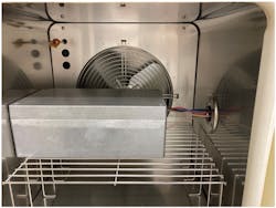
- A shield box was installed on the evaluation board inside the thermostatic chamber (Fig. 6).
- The coaxial cable connected to the noninverting input terminal was shortened to reduce the Cp (Fig. 7).
For one, we expect to reduce the effect of external noise, and secondly, we expect to reduce the small leakage current in the cable (the recalculated Cp is 35.2 pF). However, although these measures were taken and remeasured, no reproducibility was observed, similar to the results obtained in “Capacitive Integration Measurement.” The waveforms differed significantly from what was expected.
Remove the Test Box
The test box was removed, and the SW was changed by directly shorting and opening the ground (Fig. 8). In other words, the conductance component called the test box was removed and the measurement was performed. As a result, we were able to obtain the waveform as shown in Figure 9.
The output voltage measured by the DMM increased with a constant slope and reached around 4.16 V in all measurements. The corresponding current shows a value of about 50 fA.
Furthermore, the red line in Figure 9 shows the waveform of the re-measurement with a shorter coaxial cable connected to the noninverting input terminal (Cp = 26.5 pF). The slope of the voltage rise is as large as the theoretical calculation. From these measurement results, it was found that the conductance component on the input side has a significant adverse effect on measurement accuracy.
Conclusion
Although the femtoampere-level measurement can be performed in a general lab environment, the path of the leakage current on the input side of the operational amplifier needs to be carefully considered.
To improve the accuracy of the measurement, it’s recommended to use a Teflon terminal block on the input side or a triaxial cable together with the evaluation board.
Check out more articles in the TechXchange: Why Low Iq is the Smart Thing to Do
Acknowledgements
The author would like to thank Scott Hunt, Iku Nagai, and Jun Kakinuma for their technical advice.
Reference
Wong, Vicky. “AN-1373 Application Note: ADA4530-1 Femtoampere Level Input Bias Current Measurement.” Analog Devices, Inc., October 2015.
About the Author
Aoi Ueda
Field Applications Engineer, Analog Devices Inc.
Aoi Ueda joined Analog Devices Japan (ADKK) in 2021 as a field applications engineer for the Instrumentation Group. He has a master’s degree in engineering from Nara Institute of Science and Technology (2021) and a bachelor’s degree from National Institute of Technology, Nara College (2019). He is a Japanese idol otaku.
Voice Your Opinion!
To join the conversation, and become an exclusive member of Electronic Design, create an account today!

Leaders relevant to this article:


