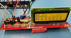
Microcontroller Controls Relays via RF Modules
Members can download this article in PDF format.
In this design idea, you will learn how to interface two PIC microcontrollers using a wireless 433-MHz RF transmitter/receiver pair to control up to six relays and monitor two analog signals. The design will find multiple applications intended for smart-home systems. The RF modules (PT2262) used in this setup are available from Digi-Key (P/N: 1597-1223-ND).
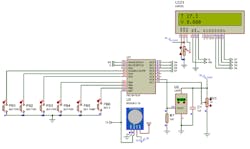
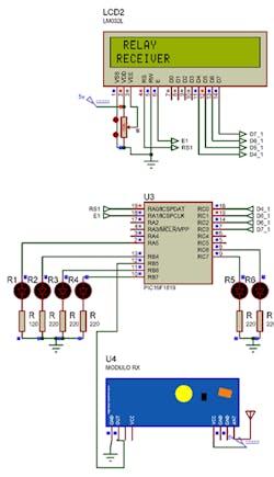
Figure 1 shows the transmitter based on the microcontroller PIC16F1619. Pushbuttons PB1 thru PB4 are enabled to control four relays in the receiver module in Figure 2.Pushbuttons PB5 and PB6 are used to set the voltage thresholds for the temperature sensor applied on input RC6, and the potentiometer connected on RC7 in the microcontroller. These two readings control Relays 5 and 6, respectively, in the receiver module. This feature can be used to operate as a thermostat in A/C systems.
PB5 and PB6 are configured to set up temperature and voltage, respectively. Temperature can be set in intervals of 1°C. The second signal that can be measured is voltage. It can be set in intervals of 10 mV, setting the maximum voltage to 4.99 V.
When setting the values of temperature and voltage, an interval is created, in which their state doesn’t change. This is called hysteresis. When the temperature increases ±1°C, the voltage changes with a resolution of 10 mV. If the voltage or temperature is within two intervals, it will remain in the last active state, either On or Off. This is used to avoid damaging the connected relays.
Listings 1 and 2 below show the code for the transmitter and receiver modules, respectively. The transmitter module displays the actual temperature detected by the LM34 sensor, and the voltage coming from the trim potentiometer. The receiver module displays the status of each relay.
This circuit uses the EUSART (Enhanced Universal Synchronous Asynchronous Receiver Transmitter) modules embedded in two PIC microcontrollers 16F1619 and 16F1614. The communication is full-duplex between both devices (Rx and Tx).
To establish communication, it’s necessary to have a starting bit for a period of time to alert the receptor that a data package is about to be transmitted. This allows the receiver clock to start synchronization with a 0 bit. Then each bit is sent individually, starting with the LSB bit through the MSB bit. Each bit has the same period. Once all bits are transmitted, it has to wait for the high-logic Stop bit to indicate end of transmission.1
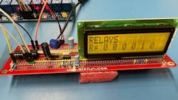
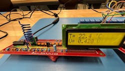
Figures 3 and 4 show the actual assembled circuits in two printed circuit boards.
Reference
1. Jimenez, Ricardo, and Alvarez, Gabriel L. “Microcontroller Sends Voltage and Frequency via Low-Cost Modules,” Aug. 12, 2020, www.electronicdesign.com.
Listing 1: Code for the Transmitter PIC16F1619
'*  Name    : Wireless RF Transmitter module code
'*  Date    : 6/10/22                                        *
'*  Version : 1.0   PIC16F1619    PBP3 compiler melabs.com
'*  Notes   :    Transmitter 4 relays;

  #CONFIG
    __config _CONFIG1,  _FOSC_INTOSC & _PWRTE_ON & _MCLRE_OFF & _CP_OFF & _BOREN_ON & _CLKOUTEN_OFF
    __config _CONFIG2,  _WRT_OFF & _PPS1WAY_OFF & _ZCD_OFF & _PLLEN_OFF & _STVREN_ON & _BORV_LO & _LVP_OFF
    __config _CONFIG3,  _WDTCPS_WDTCPS4 & _WDTE_ON & _WDTCWS_WDTCWS100 & _WDTCCS_LFINTOSC
  #ENDCONFIG
;CONFIGURATION OF THE INTERNAL CLOCK
OSCCON = %01101010; $6A, INTERN CLOCK AT 4MHZ
OSCSTAT = %00011111; $1F, INTERNAL CLOCK ENABLE
OSCTUNE = 0;INTERNAL OSC WORKS AT THE CALIBRATED FREQUENCY
; PINS CONFIGURATION
;--PORTA--
TRISA = %00111100;      RA3:RA4:RA5 AS INPUT
ANSELA = %00000100;  ALL PINS ARE DIGITAL
OPTION_REG.7=0;          PULL-UPS ENABLED
WPUA = %00111000;     RA2:RA5 PULL-UPS enabled
;--PORTB--
TRISB = %01110000;      RB4:RA5:RB6 AS INPUT
ANSELB = 0;                     ALL PINS ARE DIGITAL
WPUB = %01110000;    RB4:RA5:RB6 ENABLED PULL UPS
;--PORTC--
TRISC = %11000000;      RA6:RA7 AS INPUTs
ANSELC = %11000000;  RA6:RA7 ARE ANALOG
WPUC = 0;                       PULL UPS DISABLED
;---
INTCON = %11000000;  ENABLE ALL INTERRUPTs
;ADC CONFIGURATION
ADCON0 = %00001101;  ADC ENABLED
ADCON1 = %10000000;  RIGHT JUSTIFIED
;PIE1 = %01000000;         ENABLED ADC INTERRUPT
;--LCD CONFIGURATION ----------------------
DEFINE LCD_DREG PORTC ' THE DATA CHANNEL IS THE PORTC
DEFINE LCD_DBIT 0              ' PORTC.0 IS THE LSB
DEFINE LCD_RSREG PORTA ' RS IS CONNECTED IN PORTA.0
DEFINE LCD_RSBIT 0
DEFINE LCD_EREG PORTA ' E IS CONNECTEC IN PORTA.1
DEFINE LCD_EBIT 1
DEFINE LCD_BITS 4 ' 4 LINES OF DATA
DEFINE LCD_LINES 2 ' THE DISPLAY IS OF 2 LINES
DEFINE LCD_COMMANDUS 1500 ' 1500uS OF COMMAND TIME
DEFINE LCD_DATAUS 44 '44uS TIME OF DATA
;-----------------------------------------------------
;SERIAL PORT CONFIG
TX1STA = %00100000;        $20, ENABLE TRANSMISSION, 8 BITS, LOW VELOCITY
BAUD1CON = %00000000; NO INVERTER, DETECTION OF FALLING EDGE
SPBRGL = 25;                         CALCULATED at 2400 BPS
RC1STA.7 = 1;                        ENABLE SERIAL PORT
RB7PPS = %10010;               ACTIVATING PPS MODULE
;---------------------------------------------------------
;TIMER 1 CONFIG
T1CON = %11000101;         TIMER 1 ENABLED, LFINTOSC, 1:8 PREESCALE
;-----------------------------
;variables
ADC VAR WORD
REMAINDER VAR WORD
RELE VAR BYTE
VIN VAR WORD
VR VAR WORD
ES1 VAR BIT
ES11 VAR BIT
ES2 VAR BIT
ES21 VAR BIT
TR VAR WORD
CH VAR BYTE
VP VAR WORD
TP VAR WORD
DIR VAR WORD;
DAT VAR WORD
T VAR BYTE[4]
VD VAR BYTE[4]
X VAR BYTE
R VAR BYTE;
STATE VAR WORD;
Y VAR BYTE
TIME VAR BYTE
TMR VAR WORD
;ALIAS
PB1 VAR PORTA.3;
PB2 VAR PORTA.4;
PB3 VAR PORTA.5;
PB4 VAR PORTB.4;
PB5 VAR PORTB.5;
PB6 VAR PORTB.6;

;---INITIALIZATION--
RELE = 0;
TR = 0;
;VP = 9999;
;TP = 9999;
VR = 0;
ES1 = 0
ES2 = 0
ES11 = 1;
ES21 = 1;
FOR X = 0 TO 3
VD[X] = 0
T[X]=0
NEXT X
TIME = 250
;------
READCODE $1FF5,STATE

IF STATE = 0  THEN
    READCODE $1FF6,TP;
    READCODE $1FF7,VP;
ELSE
    VP = 9999;
    TP=  999;
    DIR = $1FF5;
    DAT = 5;
    GOSUB ERASE
    GOSUB SAVE
ENDIF
;------------
LCDOUT $FE, $80, "WIRELESS"
LCDOUT $FE,$C0, "CONTROLLER "
PAUSE 1000;
;LCDOUT $FE, $80, "your name               “
;LCDOUT $FE,$C0, "your session            "
;PAUSE 2000;

MAIN:
;R = RELE.
R.0 = PB1
R.1 = PB2
R.2 = PB3
R.3 = PB4
IF pb1 = 0 THEN; WHEN BUTTONS IS PRESSED
    PAUSE TIME
    RELE.0= 1;        INVERT STATE
    GOSUB SEND
    RELE.0 = 0;
ENDIF
IF PB2 = 0 THEN
    PAUSE TIME
    RELE.1= 1; INVERT STATE
    GOSUB SEND
    RELE.1 = 0;
ENDIF
IF PB3 = 0 THEN
    PAUSE TIME
    RELE.2= 1; INVERT STATE
    GOSUB SEND
    RELE.2 = 0
ENDIF
IF PB4 = 0 THEN
    PAUSE TIME
    RELE.3= 1; INVERT STATE
    GOSUB SEND
    RELE.3= 0;
ENDIF
IF PB5 = 0 THEN GOSUB SET_TEMP; VOLTAGE SETPOINT
IF PB6 = 0 THEN GOSUB SET_V;  TEMPERATURE SETPOINT
;GOSUB ADC_READ;
;-*---
CH = 2;      AN9 VOLTMETER, TEMP
GOSUB ADC_READ
GOSUB D_V;
VR = VIN
;--------
CH = 8;       AN8 VOLTMETER
GOSUB ADC_READ
GOSUB D_T
TR = VIN;
PAUSE 200
;-------
IF TR > TP THEN; WHEN READ TEMPERATURE IS HIGER THAN SET POINT
    ES1 = 0;
    RELE.4 = 1
ELSE
    ES1 = 1;
    RELE.4 = 0;
ENDIF
;----
IF VR>VP THEN; WHEN READ VOLTAGE IS HIGHER THAN SET POINT
    RELE.5 = 1
    ES2 = 0;
ELSE
    RELE.5 = 0
    ES2 = 1
ENDIF
;----
IF ES11 <> ES1 THEN; IF THE STATE IS DIFFERENT
    GOSUB SEND;
    ES11 = ~ES11;
ENDIF

IF ES21 <> ES2 THEN; IF THE STATE IS DIFFERENT
    GOSUB SEND;
    ES21 = ~ES21;
ENDIF
;---- display temperature and voltage ------
LCDOUT $FE,$80,"T= ",DEC T[2], DEC T[1],".",DEC T[0]," 'C"
pause 200;
LCDOUT $FE,$C0,"V= ",DEC VD[3],".",DEC VD[2],DEC VD[1],DEC VD[0]," V"
pause 500;
GOTO MAIN
;----------------
SET_TEMP:
PAUSE TIME;
        TMR1L = 0;
        TMR1H = 0;
    FOR Y = 0 TO 1
        TMR1L = 0;
        TMR1H = 0;
        TEMP_STAY:
            if PB5 = 0 THEN
                TP = TP+5; INCREMENT TEMPERATURE SET POINT BY 0.1 DEGREE
                PAUSE 150;
                Y = 0;
                IF TP > 999 THEN TP=0; IS THE SET POINT IS HIGHER THAN 99.9?
                TMR1L = 0;
                TMR1H = 0;
            ENDIF
            VIN = TP;
            GOSUB D_T
            TMR.BYTE0 = TMR1L;
            TMR.BYTE1 = TMR1H;
            LCDOUT $FE,$80,"SET TEMP"
            lcdout $fe,$c0,DEC t[2],dec t[1],".",dec t[0],"               "
        IF TMR < 31000 THEN GOTO TEMP_STAY; IF NOT ELAPSED TIME
     NEXT Y
     gosub SECUENCE
RETURN;
;----------------
SET_V:
PAUSE TIME
    FOR Y = 0 TO 1
    TMR1L = 0;
    TMR1H = 0;
        V_STAY:
            if PB6 = 0 THEN
                VP = VP + 50; INCREMENT VOLTAGE trip point BY 50 mV
                PAUSE 100;
                Y = 0;
                IF VP >4900 THEN VP = 0; IF trip point IS HIGHER THAN 4.9V
                TMR1L = 0;
                TMR1H = 0;
            ENDIF
            VIN = VP
            GOSUB D_V;
            LCDOUT $FE,$80,"SET VOLTAGE"
            lcdout $fe,$c0,DEC VD[3],".",dec VD[2],dec VD[1],DEC VD[0],"                 "
            TMR.BYTE0 = TMR1L;
            TMR.BYTE1 = TMR1H;

        IF TMR< 31000 THEN GOTO V_STAY;  IF NOT ELAPSED THE TIME
     NEXT Y
     GOSUB SECUENCE
RETURN
;----------------
ADC_READ:
    CH = CH<<2;
    ADCON0 = CH^%10000001; BITWISE XNOR
    PAUSE 1
    ADCON0.1 = 1;
    ;PAUSE 1;    ENABLE ADC MODULE IN PIC
    HERE1: IF ADCON0.1 = 1 THEN HERE1; wait for conversion bit
    ADCON0.0 = 0;
    ADC.BYTE0 = ADRESL;     SAVE LOWER REGISTER ADC IN VARIABLE VIN
    ADC.BYTE1 = ADRESH;     SAVE HIGHER REGISTER ADC IN VARIABLE VIN
    REMAINDER = ADC*4887; MULTIPLYING BY RESLSB = 4.8887
    VIN = div32 1000;              PERFORM 16-BIT DIVISION
return
;-------
D_T:
  FOR X = 0 TO 3; OBTAIN THE DIGITS
    T[X]= VIN DIG X
    NEXT X
RETURN
;---
D_V:
    FOR X = 0 TO 3; OBTAIN THE DIGITS
        VD[X]= VIN DIG X
    NEXT X
RETURN

;----
SEND:
for x = 0 to 2
    HSEROUT ["R",DEC X,RELE] ; SEND DATA IN SERIAL PORT
next x
RETURN
;-------
UNLOCK:             ; UNLOCK SEQUENCE
    ASM
        BANKSEL PMCON2
        MOVLW 0x55
        MOVWF PMCON2 & 0x7F
        MOVLW 0xAA
        MOVWF PMCON2 & 0x7F
        BSF PMCON1 & 0x7F,1 ; set WR bit
        NOP
        NOP
    ENDASM
RETURN
;----------
ERASE:                ;required sequence
    PMCON1.4 = 1;
    PMCON1.2 = 1;
    GOSUB UNLOCK;
    PMCON1.2=0;
    PMCON1.4=0;
RETURN
;
SECUENCE:         ;data save sequence
    GOSUB ERASE
    DIR = $1FF5
    DAT = 0;
    GOSUB SAVE
    DIR =$1FF6;
    DAT = TP;
    GOSUB SAVE;
    DIR =$1FF7
    DAT = VP
    GOSUB SAVE
RETURN

SAVE:                 ;instruccion set
    PMADRL = DIR.BYTE0;
    PMADRH = DIR.BYTE1;
    PMDATL= DAT.BYTE0;
    PMDATH= DAT.BYTE1;


    PMCON1.6 = 0;
    PMCON1.5 = 0;
    PMCON1.4 = 0;
    PMCON1.2 = 1;
    PMCON1.1 = 1;
    PMCON1.0 = 0;
    GOSUB UNLOCK;
    STAY:IF (PMCON1.1 = 1) AND (PMCON1.3 = 1)THEN STAY;
    IF PMCON1.3 = 1 THEN save;
    PMCON1.6=0;
    PMCON1.5=0;
    PMCON1.1=0;
    PMCON1.2=0;

RETURN;
Listing 2: Code for the Receiver Unit Using a PIC16F1619
'*  Name    :
'*          :  pic16f1619 pbp3 compiler from melabs.com
'*  Date    : 6/10/22                                        *
'*  Version : 1.0                                               *
'*  Notes   :    Receiver for 6 relays;
  #CONFIG
    __config _CONFIG1,  _FOSC_INTOSC & _PWRTE_ON & _MCLRE_OFF & _CP_OFF & _BOREN_ON & _CLKOUTEN_OFF
    __config _CONFIG2,  _WRT_OFF & _PPS1WAY_OFF & _ZCD_OFF & _PLLEN_OFF & _STVREN_ON & _BORV_LO & _LVP_OFF
    __config _CONFIG3,  _WDTCPS_WDTCPS4 & _WDTE_ON & _WDTCWS_WDTCWS100 & _WDTCCS_LFINTOSC
  #ENDCONFIG

; INTERNAL CLOCK configuration
OSCCON = %01101010; $6A, INTERN CLOCK AT 4MHZ
OSCSTAT = %00011111; $1F, INTERNAL CLOCK ENABLE
OSCTUNE = 0;INTERNAL OSC WORKS AT CALIBRATED FREQUENCY
; PINS CONFIGURATION
;--PORTA--
TRISA = 0; RA4 INPUT, all other are outputs
ANSELA = 0; RA4 ANALOG, all other are digital
OPTION_REG.7=0;  pull-ups control
WPUA = 0; PULL-UPS Disabled
;--PORTB--
TRISB = %00100000;
ANSELB =
WPUB = 0; PULL UPS DISABLED
;--PORTC--
TRISC = 0; portc set to outputs
ANSELC = 0; digital port
WPUC = 0; PULL UPS Disabled
;---
PORTC = 0
PORTB = 0
PORTA = 0
PAUSE 1000;
;--LCD CONFIGURATION ----------------------
DEFINE LCD_DREG PORTC ;DATA CHANNEL IS PORTC
DEFINE LCD_DBIT 0 ' PORTC.0 IS THE LSB
DEFINE LCD_RSREG PORTA ' RS IS CONNECTED IN PORTA.0
DEFINE LCD_RSBIT 0
DEFINE LCD_EREG PORTA ' E IS CONNECTED IN PORTA.1
DEFINE LCD_EBIT 1
DEFINE LCD_BITS 4 ' 4 DATA lines
DEFINE LCD_LINES 2 ' DISPLAY IS 2 LINES
DEFINE LCD_COMMANDUS 1500 ' 1500uS COMMAND TIME
DEFINE LCD_DATAUS 44 '44uS  DATA time
;------SETTING UP LCD------------------------------------------------
LCDOUT $FE,$28;  $28 FUNCTION SET, 4 BITS
LCDOUT $FE,$10;  $10 SHIFT DISPLAY
LCDOUT $FE,$0C;  $0C DISPLAY ON
LCDOUT $FE,$06;  $06 ENTRY MODE SET
;-------------------------------------------------------------------------------
;SERIAL PORT config
RC1STA = %10010000; ENABLED SERIAL PORT
BAUD1CON = %00000000; NO INV, FALLING EDGE detection
SPBRGL = 25; CALCULATED OF 2400 BPS
RXPPS = %01101
DEFINE HSER_CLROERR 1; CLEAR OVERRUN ERROR
;---------------------------------------------------------
LCDOUT $FE,$80," WIRELESS RELAY "
LCDOUT $FE,$C0,"    RECEIVER    "
PAUSE 5000;
; VARIABLES------
RELE VAr byte;
B VAR BYTE;
ANT VAR BYTE;
STATE VAR BYTE
x var byte
;---ALIAS
RE1 VAR PORTA.5
RE2 VAR PORTB.4
RE3 VAR PORTB.6
RE4 VAR PORTB.7
RE5 VAR PORTC.6
RE6 VAR PORTC.7
;---------
STATE = 0;
;-----
MAIN:
HSERIN [WAIT("R2"),rele]
IF RELE.0 = 1 THEN RE1 = ~RE1
IF RELE.1 = 1 THEN RE2 = ~RE2
IF RELE.2 = 1 THEN RE3 = ~RE3
IF RELE.3 = 1 THEN RE4 = ~RE4
;RE1 = STATE.0
;RE2 = STATE.1
;RE3 = STATE.2
;RE4 = STATE.3
RE5 = RELE.4
RE6 = RELE.5
lcdout $fe,$80,"RELAYS          "
lcdout $fe,$C0,"R= ",bin re6," ",bin re5," ",bin re4," ",bin re3," ",bin re2," ",bin re1;
pause 300;
GOTO MAIN
END
About the Author
Ricardo Jimenez
Ricardo Jimenez holds a master's degree in electronics from the Instituto Tecnologico de Mexicali.
Voice Your Opinion!
To join the conversation, and become an exclusive member of Electronic Design, create an account today!

Leaders relevant to this article:
