Triple-level-cell (TLC) NAND is the mainstay for high-capacity flash storage. Storing three bits per cell boosts the amount of information that can be handled by a single chip. However, there are tradeoffs: A cell can handle only so many writes, and packing more data into a cell—and chip—increases the number of errors. Forward-error-correcting (FEC) technology, though, along with other flash-management support, helps improve system reliability.
TLC NAND systems are already taking advantage of 64-layer 3D technology. This is how vendors are able to deliver multi-terabyte solid-state drives (SSD) and terabyte M.2 modules.
The technology continues to advance, as one of the hot topics at the Flash Memory Summit will be 4-bit QLC NAND flash. QLC flash works with existing 3D technology, essentially doubling the available storage.
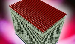
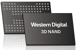
Western Digital’s 3D QLC flash-memory chips double storage capacity.
Western Digital and Toshiba have already announced their QLC BiCS flash-memory chips (see figure). The 768-Gbit (96-Gbyte) die capacity improves on the 512-Gbit TLC chips. A 16-die stack of the TLC chips provide 1 Tbyte of storage.
The 1-bit, single-level-cell (SLC) and 2-bit multilevel cell (MLC) still have their place, especially in embedded applications. And TLC will not go away. The fact is that it will take time for QLC to become the dominant technology for high-capacity drives. Developers and enterprise manager will still need to consider the cost/performance equation for their storage devices.
If you’re considering QLC NAND, there’s another benefit that awaits: The higher-capacity drives will make it easier to provide configurable over-provisioning that’s already available on high-capacity SSDs like Micron’s FlexPro drives.
About the Author
William G. Wong
Senior Content Director - Electronic Design and Microwaves & RF
I am Editor of Electronic Design focusing on embedded, software, and systems. As Senior Content Director, I also manage Microwaves & RF and I work with a great team of editors to provide engineers, programmers, developers and technical managers with interesting and useful articles and videos on a regular basis. Check out our free newsletters to see the latest content.
You can send press releases for new products for possible coverage on the website. I am also interested in receiving contributed articles for publishing on our website. Use our template and send to me along with a signed release form.
Check out my blog, AltEmbedded on Electronic Design, as well as his latest articles on this site that are listed below.
You can visit my social media via these links:
- AltEmbedded on Electronic Design
- Bill Wong on Facebook
- @AltEmbedded on Twitter
- Bill Wong on LinkedIn
I earned a Bachelor of Electrical Engineering at the Georgia Institute of Technology and a Masters in Computer Science from Rutgers University. I still do a bit of programming using everything from C and C++ to Rust and Ada/SPARK. I do a bit of PHP programming for Drupal websites. I have posted a few Drupal modules.
I still get a hand on software and electronic hardware. Some of this can be found on our Kit Close-Up video series. You can also see me on many of our TechXchange Talk videos. I am interested in a range of projects from robotics to artificial intelligence.


