Monolithic Switching Regulator: When Everything is on a Chip
A switching regulator can be constructed either monolithically or via a controller. In a monolithic switching regulator, the respective power switches, usually MOSFETs, are integrated within a single silicon chip. With controllers, in addition to the controller IC, the power semiconductors must be selected and positioned separately.
MOSFET selection is time-consuming and requires a certain understanding of the parameters of a switch, something designers needn’t deal with when using a monolithic design. Also, controller solutions usually take up more space on the board than highly integrated solutions.
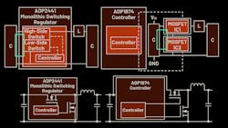
Thus, it’s no wonder that over the years, ever-more switching regulators have been executed monolithically. Today, there’s a large selection of suitable solutions available, even for higher power. Figure 1 shows a monolithic buck converter on the left and a controller solution on the right.
Monolithic Regulator vs. Controller
While monolithic solutions require less space and the design process is simplified, one advantage of a controller solution is more flexibility. A designer can select optimized, application-specific switches for a controller solution, and there’s access to the gate for the switches, enabling the switching edges to be influenced with clever employment of passive components. Furthermore, controller solutions are fit for high power since large discrete switches can be selected and switching losses dissipate with thermal separation from the controller IC.
However, in addition to these well-known arguments for and against a monolithic solution, another aspect often isn’t considered. In switching regulators, the so-called hot loops are decisive for low radiated emissions. In all switching regulators, the EMC should be optimized as much as possible. One of the basic rules for accomplishing this is to minimize the parasitic inductances in the respective hot loop.
In a buck converter, the path between the input capacitor and the high-side switch, the connection between the high-side switch and the low-side switch, and the connection between the low-side switch and the input capacitor, are part of the hot loop. They’re the current paths in which a current flow changes at the speed of the switching transitions. Through the rapid current changes, a voltage offset forms via a parasitic inductance and can couple into different circuit segments as interference.
Thus, these parasitic inductances in the hot loops must be kept as low as possible. Figure 2 shows the paths of the respective hot loop (in red) for a monolithic switching regulator on the left and for a controller solution on the right. We can see there are two advantages with the monolithic solution.
First, the hot loop is smaller than that for the controller. Second, the connection path between the high-side switch and the low-side switch is very short and only routed on the silicon. In comparison, for a solution with a controller IC, this connected current path must be routed through the parasitic inductance of the packaging, usually with parasitic inductance from bonding wires and lead frames. This causes a higher voltage offset and, accordingly, poorer EMC behavior.
As a result, monolithic switching regulators offer an additional, lesser-known advantage with respect to EMI. How high this interference is and how it affects a circuit depends on many other parameters. The basic idea that there’s a difference between monolithic switching regulators and solutions with controller ICs in terms of EMC behavior is worth considering, though.
Frederik Dostal is a Field Applications Engineer at Analog Devices.
About the Author

Frederik Dostal
Power-Management Technical Expert
Frederik Dostal is a power-management expert with more than 20 years of experience in this industry. After his studies of microelectronics at the University of Erlangen, Germany, he joined National Semiconductor in 2001, where he worked as a field applications engineer, gaining a lot of experience in implementing power-management solutions in customer projects. During his time at National, he also spent four years in Phoenix, Arizona (USA), working on switch-mode power supplies as an applications engineer.
In 2009, he joined Analog Devices, where since then he held a variety of positions working for the product line and European technical support, and currently brings in his broad design and application knowledge as a power-management expert. Frederik works in the ADI office in Munich, Germany.
Also check out my:


