What’s the Difference Between Optical and Electrical Technology for 100-Gbit/s Connectivity in Future Systems?
High-throughput network switches and high-performance computing systems have maintained their exponential growth for the past 20 years and will continue to do so into the foreseeable future. While the performance and bandwidth of these systems have almost doubled over the past two decades, most if not all of such improvements in the first decade were due to higher transistor speeds and greater integration of CMOS technology.
Over the past 10 years, though, improvements in transistor performance have slowed down with marginal power improvements from one process node to another, limiting the integration density. Multicore parallel architectures have been employed to keep up with the demand.
This file type includes high resolution graphics and schematics when applicable.
Interconnect technology is essential in enabling these new parallel architectures to achieve their targeted performance. Limitations in the interconnect throughput, density, and latency pose a major bottleneck to the system performance, hindering further advances for future architectures.
Optical and electrical interconnect technologies have always competed to be the solution of choice. Each offers specific tradeoffs based on density, reach, reliability, cost, and power in a given application.
System manufacturers historically have been reluctant to replace incumbent electrical interconnects with optical solutions, due to their lower complexity and lower-cost supply chain, unless the lack of a viable electrical solution has made it necessary. In most generations of high-performance systems, optics seem to take over at first, but the cost advantage of their electrical counterparts wins in the end. Therefore, optical interconnects have usually ended up to be limited to longer-distance links where the attenuation in copper cable is too high for the electrical circuits to compensate.
With the performance requirements in future systems and new interconnect technologies, other factors may come into the decision-making process that can affect the old paradigms. Examining the tradeoffs of the electrical and optical interconnect solutions based on different system requirements and configurations serves as a framework for the selection of proper interconnects in next-generation systems.
Interconnect Selection Considerations
The adoption of interconnect technology is always driven by the application and usage model. Many factors are involved in the selection of the best solution that meets all system requirements. One must consider key factors in the selection process to ensure an optimized solution for a target application.
Throughput per device (Gbits/s/chip) is the aggregate throughput of transmitter plus receiver bandwidth that can be integrated in a single device or chip. Currently, it is feasible to build an electrical device with 200 25-Gbit/s transmitters and receivers to support 10-Tbit/s aggregate throughput. The maximum throughput per device is limited by the area and power per transceiver, as that dictates the number of transceivers on a silicon device.
A large transceiver area can limit the number of cores to be integrated on a single chip before the chip area exceeds the process yield curve, making it uneconomical or even impractical to manufacture. Optical solutions also carry the burden of optical functions that claim their additional area, whether they’re partly integrated in ASICs like silicon photonics or as off-chip components on printed-circuit boards (PCBs) that further limit the effective density.
On the other hand, given the packaging and system cooling required to stay below the device maximum operating temperature, the maximum heat the device can dissipate limits its total transceiver power. Operating electrical or optical components beyond their permissible temperature range will cause them to run into short-term or long-term reliability problems.
Throughput per pin (Gbits/s/pin) measures the throughput per pin of a device or per cable. For example, to transmit 100 Gbits/s, one solution may use 10 cables each running 10 Gbits/s, while another solution may use four cables at 25 Gbits/s. In a half-duplex scenario, with both transmit and receive links, the former will take 20 cables and the latter will take eight cables, half to transmit and half to receive 100 Gbits/s. This metric is critical in high-throughput devices or systems as the large number of pins or cables is not practical to manage within a device or system.
Throughput-distance product (Gbps.meter) is a metric used to evaluate the performance of the throughput-distance or bandwidth-distance product.1 This is the link effective bandwidth per pin multiplied by the distance it can transmit the signal over a certain medium at a target bit error rate (BER). This metric is mostly a constant for any given interconnect technology, i.e., signaling technique and the medium.
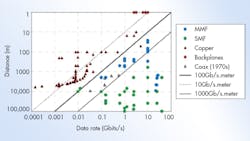
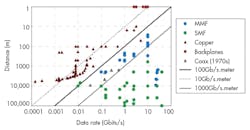
Optical communication solutions always offer a higher Gbps.meter compared to their electrical counterparts due to the superior bandwidth of optical fibers. So in applications where electrical technologies fail to deliver the required Gbps.meter, optics remains the only option. Based on three decades of commercial data, the crossover threshold where optical links hold an advantage over electrical links happens to be at the 100Gbps.meter mark (Fig. 1).2
Of course, Gbps.meter is a direct function of the transmission medium and signal processing techniques employed. With the advances in integration and speed of CMOS technology, digital signal processing (DSP) techniques can be employed to improve link performance and extend the signal reach. For example, 10GBASE-T that uses advanced signal processing techniques breaks the norm for electrical links to deliver 500Gbps.meter, as it employs four 100-m twisted-pair cables to deliver full-duplex 10 Gbits/s.
From the point of view of the transmission medium, a typical PCB trace using FR4 material provides about an order of magnitude lower Gbps.meter compared to most copper cables (e.g., twisted-pair, twinax), as they exhibit significant frequency-dependent die-electric loss, which is minimal in cables.
Similarly, a multi-mode fiber (MMF) available Gbps.meter is one to two orders of magnitude less than that of a single-mode fiber (SMF). Multi-mode optical dispersion corrupts transmitted light pulses at much lower frequencies than the dominant dispersion sources in SMF such as chromatic and polarization dispersion. In applications where electrical links can meet the required Gbps.meter, optical interconnects must provide differentiating advantages to win the sockets.
The most important metric captures the total cost of a solution for a given throughput. Lower total cost always wins in the market. The cost element has multiple factors, though, such as manufacturing/components cost, ease of deployment, power consumption, and backward compatibility. Optical solutions also always carry the additional cost of optical substrates, lenses, lasers, photodiode arrays, driver and receiver chips, connectors, and associated cooling components, which is non-existent in electrical links.
On the other hand, the integration of as much functionality on a single chip as possible, the so called system-on-chip (SoC), is leading to more compact and economical solutions. A single-chip solution can offer several advantages over a hybrid one such as less complicated packaging and assembly, ease of production testing, a smaller footprint within a system, and the elimination of interface I/Os between chips, all of which lead to a lower-cost solution.
All electrical solutions benefit from the high level of integration available in CMOS technology to be placed on the same chip as the ASIC, while the optical counterparts will need to be coupled with the optical components placed outside the ASIC. Optical technologies such as silicon photonics can integrate most of the optical functions on chip, but key optical components like the laser still will have to stay off the chip for cooling purposes.
For optics to enter high-volume mainstream applications, many believe the total cost of a link transceiver must reach a bandwidth-cost target below $1/Gbit/s, which is where electrical links are already.
Furthermore, the power consumption of a transceiver (optical or electrical) must be computed end to end between the interfaces of the core logic connected to the transmitter and the receiver. Both technologies require the serializer and deserializer (SERDES) electrical circuitry to convert the logic parallel data into the serial line rate for transmission.
Optical solutions include the additional power for the optical devices between the SERDES and the fiber, such as a laser driver, transimpedance amplifier (TIA), and limiting amplifier (LA), leading to 9 to 13 mW/Gbits/s for speed below 20 Gbits/s.2 This mW/Gbits/s goes up exponentially at higher speeds.
Electrical links, however, mostly require equalization circuitry to overcome the copper high-frequency losses in the channel or additional processing such as forward-error correction (FEC) to improve link signal-to-noise ratio (SNR) in the presence of strong interference noise. Depending on the level of signal conditioning required, electrical links may use 2 mW/Gbits/s for insertion loss compensation3 to 6 mW/Gbits/s for channels with harsh interference requiring Reed-Solomon (RS) forward error correction (FEC).4
A higher-power solution demands a better cooling and heat dissipation capability, and a better cooling mechanism translates into more cost. As a result, at the same power consumption, an electrical solution that can operate from –40°C to 125°C should be compared favorably over an optical solution with an operating temperature limited to 0°C to 70°C as far as system thermal management costs are concerned. For example, a 10-Gbit/s SERDES with 34dB IL equalization consumes 120 mW and operates up to 125°C, while a 10-Gbit/s vertical cavity surface-emitting laser (VCSEL) over 100-m fiber requires 250 mW and has to be cooled down to 70°C.
Interconnect reliability is a key concern, especially in high-performance systems with many links. Even a single failure can cause a network failure that cannot be managed without downtime. Optical links inherently are exposed to more points of failure due to the additional components used to convert electrical signals to optical and vice versa. For example, high temperatures increase the laser fail rate, which is a major reliability concern in high-performance systems that dissipate high heat and have many interconnects.
Such reliability concerns lead to requirements for controlled cooling, in some cases water cooling, to ensure the operating temperatures of the system stay below a critical threshold level. The interconnect medium is another source of reliability concerns.
For electrical links at speeds beyond 10 Gbits/s/pin, any discontinuity in the channel including wire twist and bad connectors leads to degradation in signal quality and, in severe cases, loss of link. In optical links, even small misalignments in the connectors due to unexpected movements can lead to bad optical coupling and, thus, loss of link. Misalignment is more significant for silicon photonics links using single-mode fiber with a ~1-µm alignment requirement.
Optical connectors are another point of failure. They are sensitive to dirt particles stuck in between the connection points that degrade the optical coupling between fibers, which is not a concern in electrical counterparts.
Optical Interconnects
Optical interconnects are always the solution of choice when electrical links run out of fuel to deliver the required bandwidth-distance product, which has been at the 100Gbps.meter mark for most electrical interconnect technologies for the past 30 years. For short distances, below 100 meters, optical interconnect technologies are not limited by the optical medium, but only by the bandwidth of the exploited optical Tx/Rx devices and the electronic SERDES circuitry. As the most important optical component, lasers play a key role in determining the performance and economics of the optical links.
VCSEL laser technology using multimode fibers provides fairly low-cost, low-power integration into compact arrays over distances of 100 to 300 m. Since its introduction, the technology has been a favorite choice for optical interconnects in cost-sensitive datacom applications with distances in the range of about 100 m. Inter-system connectivity, specifically rack-to-rack cluster fabrics, have benefited from the parallel optical link using such technology.
Furthermore, multimode VCSELs are much more alignment-tolerant compared to alternatives such as edge-emitting single-mode lasers, which significantly reduces the complexity of testing and installation in the system. While VCSEL transceivers have provided approximately 10-Gbit/s speeds for several years already, higher-speed VCSELs are already in development specifically for 100-Gbit/s Ethernet (100GE) that runs 25 Gbits/s on four parallel links.10
Although the 850-nm wavelength for VCSEL links has been the dominant option since the introduction of 1-Gbit/s Ethernet in 1998, some argue the optimum wavelength should be in the range of 900 to 110 nm as VCSELs at these wavelengths can operate at higher speeds and be more power efficient, more reliable, and low risk for eye safety. In addition, longer wavelengths ease the implementation of coarse wavelength division multiplexing (CWDM), which helps reduce the number of connectors and fibers by combining multiple links into a single fiber and connector.11
However, the optical losses tend to be high at longer wavelengths for polymer waveguides used in optical PCB technology, which is the favorite choice for optical backplanes and the path to high integration. The economics of scale also are important, as they play a significant role to reduce the price per port of a certain technology and transition for wide adoption.
VCSELs have been the incumbent low-cost optical interconnect for the very same reason. In the long term, though, this advantage will be eroded because of hurdles they face for integration into ASICs. Since lasers are an integral part of the VCSELs, they cannot be densely integrated into a chip unless there is good thermal control, which goes against the main advantage of VCSELs—low cost.
The drive for higher integration and the rapid increase in the cost of fiber and fiber management have motivated system designers to consider optical PCB technology based on the polymer waveguides that may provide a combination of lower cost, higher module density, and better integration.12-14 The idea behind this technology is to provide a solution with characteristics of PCBs that are cheaper than cables/fibers, eliminate fiber management hassles, and provide high-density integration within the system.
Figure 2 shows the construction of an optical module on a backplane using polymer waveguides on a flexible substrate. The laser driver, TIA, photodiode, and VCSEL are all soldered to a substrate. Holes in the substrate allow optical access to the underlying waveguide through the lens array.
This configuration is considered one of the early offerings of optical backplanes, but the waveguides within the PCB itself will be moved. However, this technology still has many hurdles to overcome, including but not limited to polymer and connector loss, low yield and reliable manufacturing, and creation of an infrastructure to allow wide adoption of this technology.
Another optical technology that has been around since the 1980s but started to make lots of noise in recent years is silicon (Si) photonics. It may offer the ultimate integration capacity with low cost by using popular CMOS technology to fabricate most optical functions on an IC. It uses on-chip optical detectors and modulators to module the light from a continuous-wave (CW) single-mode laser.15,16
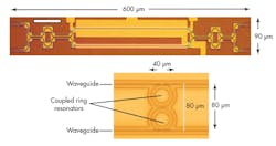
The modulators are based on a Mach-Zehnder interferometer (MZI) or a ring resonator (Fig. 3). The MZI modulators offer approximately 100 times larger optical bandwidth and low temperature sensitivity, but at the cost of about 20 times more area and more than twice the power compared to the ring resonators.
To reduce chip area and cost by using the significantly smaller ring resonators, the temperature must be well controlled for proper optical modulation. This is less of a concern in high-performance systems using water cooling. Si photonics that use low-cost ring resonators, though, run into a challenge in mainstream systems where fancy cooling is considered too expensive to be an option.
The technology requires the use of single-mode fiber and longer wavelengths of 1300 to 1500 nm to be in a region where silicon is transparent. As a result, Si-photonics-based transceivers are incompatible with the shorter wavelength and multimode technology based on VCSELs, and they cannot interoperate with VCSEL-based systems. However, the single-mode nature of these interconnects allows longer lengths up to 2 km, making them a favorite solution for being scalable to large installations.
Packing in Si photonics is a topic that is usually neglected in tradeoff discussions for the technology. While the Si photonics chip itself is relatively cheap, the coupling of the chip to the 9-µm SMF with 1-µm alignment tolerance and the separate CW single-mode laser can end up adding significant cost to the whole solution. For example, the throughput of passive alignment with pick-and-place machines goes down from 20,000 units/hr with 10-µm tolerance for MMF to just 200 units/hr with 1-µm tolerance required for SMF.
The laser can be integrated on chip for higher integration and lower cost. But in this scenario, to ensure a stable light wavelength, an even better cooling system is needed to control laser temperature exposed to direct heat from the chip. Further adding to the cost is the need for optical isolators since single-mode edge-emitting lasers are more sensitive to reflected light than multimode VCSELs.
Total power consumption must be a primary consideration for optical solutions in general. As discussed earlier, optical links may not need any equalization to deliver up to 500Gbps.meter thanks to significant fiber bandwidth. However, the optical components sitting between the electronic SERDES and the fiber consume a considerable portion of the overall link power, and their mW/Gbits/s increases with link speed as well.
For example, just the TIA power for a 25-Gbit/s optical link is about 70 mW5, and the whole optical to electrical conversion on the receive side at 25 Gbits/s can consume more than 120 mW.6 Similar power consumption numbers are expected at such speeds on the transmit side with the pre-amplifier, laser driver, and laser power itself.
For the Si photonics technology, some of the optical circuitry could have very low power consumption (e.g., modulator power can be in the approximately 100-fJ/bit range17). Yet designs with a practical balance of performance and temperature control, accounting for all power sources (e.g., temperature control and CW laser) may find that such a potential advantage is significantly fading.
Electrical Interconnects
State-of-the-art electrical interconnects now being designed into emerging systems deliver an effective data rate of 25 Gbits/s/pin to 32 Gbits/s/pin.5-9 IEEE Standard 802.3bj for 100-Gbit/s Ethernet (100GE) is an example of industry recent efforts to address future system interconnect needs by defining four 25-Gbit/s/pin interconnects over electrical channels. In this scenario, 100 Gbits/s is transmitted over four differential channels in either direction, leading to a total of eight differential channels (or 16 conductors) for a bi-directional 100-Gbits/s link.
Transmission over backplane PCB traces is the preferred choice for intra-system connectivity as it eliminates the messy and bulky cable management that leads to high cost and reliability issues by itself. As a result, IEEE 802.3bj has defined two signaling standards targeted for backplanes: a conventional PAM2 signaling standard named 100GBASE-KR4 and a PAM4 signaling standard named 100GBASE-KP4.
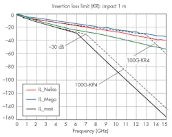
Both standards define serial communication over a copper backplane with about 30 dB of insertion loss (IL) at the corresponding Nyquist frequencies, approximately 12.5 GHz for KR4 and about 6.5 GHz for KP4. 100GBASE-KR4 has received more tracking in the industry so far, as IC designers and system architects have designed for conventional PAM2 signaling for decades due to its inherent simplicity. However, PAM2 is quickly failing to deliver a desirable bandwidth-distance product over copper for speeds well above 10 Gbits/s/pin.
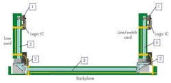
A typical electrical backplane consists of line cards with transceiver-embedded ASICs, array vertical connectors, and the backplane connecting the line cards (Fig. 4). The IL of the PCB traces on the line cards and backplane first distort the electrical signals traveling through the backplane. The other sources of signal degradation are signal return loss (RL) due to discontinuity in the path and crosstalk from adjacent lanes. Signal processing techniques such as continuous-time linear equalization (CTLE) and decision feedback equalization (DFE) mostly compensate for signal losses such as IL and RL.
Interference noise sources, such as those from adjacent channels, degrade the link SNR and can be addressed by forward error correction (FEC) algorithms such as Reed-Solomon (RS FEC) that can provide up to 6 dB of SNR gain. FECs inherently come with a latency penalty. While there are implementation techniques to reduce the latency of a RS decoder below 100 ns in existing advanced CMOS nodes, such latency may still not be acceptable for certain applications. Alternatively, other DSP techniques can be employed to improve link SNR to directly measure and cancel the crosstalk in the link with negligible latency penalty.
Figure 5 shows the IL limit lines for the two 100GE backplane standards as well as the IL of 1-m PCB over different types of materials. For example, a loss of 30 dB at 12.5 GHz translates to about 0.5 m of FR4 trace. 100GBASE-KR4 can provide a bandwidth-distance product limited to approximately 12.5 Gbps.meter on a FR backplane, then, while this metric for 100GBASE-KP4 using PAM4 almost doubles to 25Gbps.meter.
Of course, replacing FR4 with more expensive PCB material such as Nelco4000 or Megtron6 will reduce die-electric loss from almost 30% to as much as 50%. Such superior materials help extend the copper backplane reach up to 1 meter for the popular PAM2 signaling. In addition to higher inherent cost, though, they are not as durable and robust as FR4 material.
The IEEE task force 100GBASE-CR4 proposes using similar signaling to 100GBASE-KR4 over copper cables for longer reach. The IL figure for copper cable generally is about an order of magnitude lower than basic PCB materials, extending the reach for PAM2 signaling to at least 5 m, effectively providing a bandwidth-distance product over 125Gbps.meter.
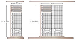
The copper cable in 100GBASE-CR4 comprises of a group of eight twinax cables bundled together to provide four differential channels in either direction for bi-directional operation. Electrical cable solutions are dominantly deployed for inter-systems connectivity either within the same rack or between racks, where there are fewer interconnects but a connection distance of less than 1 m is required. Figure 6 shows two scenarios that represent most of the rack configurations in data centers, where a 5-m interconnect meets the connectivity requirements in most cases.
The highest Gbps.meter in electrical solutions, however, has been offered by 10GBASE-T technology, which can drive full-duplex 10 Gbits/s over at least 100-m CAT6A cable. CAT6A cabling consists of four unshielded twisted pairs (UTPs) bundled together, each pair running an aggregate 5 Gbits/s or 2.5 Gbits/s in each direction. As a result, 10GBASE-T signaling technology leads to an effective 500Gbps.meter/pin.
Scaling the similar signal processing technology to build a 100-Gbit Ethernet link, one can potentially achieve 100 Gbits/s over approximately 20 m of a CR4 cable (i.e., eight twinax cables), or alternatively 100 Gbits/s over 5 m of a basic CR cable (i.e., two twinax cables), which is the dominant cable type used in data centers today for 10-Gbit Ethernet connectivity.
Applying similar signaling technology to basic PCB materials such as FR4 with channel bandwidths an order of magnitude lower than cables produces the bandwidth-distance product of 50Gbps.meter. Alternatively, if system designers choose a better quality material for next-generation systems, such as Megtron6, the bandwidth-distance product is extended to 100Gbps.meter. This provides a Gbps.meter that is four times what the latest electrical technology going into high-end future systems like 100GBASE-KR4 can offer.
Of course, the power of a full 10GBASE-T transceiver with an advanced DSP engine is reported to be 2.5 W in 28-nm CMOS, effectively 250 mW/Gbits/s. However, this large increase in power is due to the numerous losses, interferences, and non-idealities that exists in 100-m crude UTP cable that pushes the channel capacity less than 2 dB from the theoretical limit.
For example, the 10GBASE-T transceiver has to compensate for losses with several connectors in the path, impedance mismatches along the path, and numerous interference sources, including all adjacent UTP cables, cell phones, walkie-talkies, and all the other RF radiating sources in the system generating interference in unshielded cable.
Communication channels like twinax cables or PCB trace provide a better medium since they are well isolated from external interferences by their conducting metal shield. Furthermore, the impedance along the channel can be well controlled over a short length, and the number of discontinuities in the path usually does not exceed one or two. Such improvements in the channel quality, and thus link SNR, significantly help to reduce the DSP complexity to achieve 500Gbps.meter over shielded twinax cables or 100Gbps.meter over backplane at a reasonable power and area.
For example, to perform forward-error correction in 10GBASE-T, a low-density parity-check (LDPC) FEC is required to provide about 9 dB of SNR gain burning about 250 mW in 28-nm CMOS. In a more relaxed link with 3-dB more SNR margin, one could employ Reed-Solomon FEC such as RS (255,239) to gain approximately 6 dB of SNR gain burning about 50 mW at 10 Gbits/s,4 effectively reducing power by 80% due to simply 3-dB higher signal SNR in the channel.
Conclusion
Due to lower-volume and more costly supply chain as well as higher implementation complexity involving additional optical components, tight alignments, special packaging, and controlled cooling systems, designers have had little desire to replace incumbent electrical solutions with optics as long as electrical links can provide the required system bandwidth-distance product.
As a result, optical links have historically proven to be the dominant interconnect of choice for applications needing 100Gbps.meter and beyond. Electrical links have been the preferred choice below this threshold. The 100-Gbps.meter crossover between electrical and optical interconnects has been a good guideline capturing many commercial decisions over past three decades. However, it is an empirical observation, not a hard physical limit predicted by information theory.
Advanced CMOS process nodes have enabled electrical transceivers to operate close to the theoretical limit of the channels by incorporating advanced signal processing techniques at practical area and power numbers. For the first time in history, electrical interconnects are breaking the historical 100Gbps.meter threshold past 500Gbps.meter and approaching 1000Gbps.meter.
10GBASE-T is a good example that delivers at least 500Gbps.meter over basic copper cables. A similar technology can be employed to run up to 100 Gbits/s over approximately 20 m of a CR4 copper cable or 1 m of a backplane PCB trace.
With advances in IC process technology moving into faster and more power efficient FinFet devices, experts say that electrical interconnects may remain in data centers and communications chassis well beyond 2020.18
References
1. Ashok V. Krishnamoorthy, et al., “Progress in low-power switched optical interconnects,” IEEE Journal of Selected Topics in Quantum Electronics, March/April 2011
2. Marc A. Taubenblatt, “Optical interconnects for high-performance computing,” IEEE Journal of Lightwave Technology, February 15, 2012
3. Sameh Ibrahim and Behzad Razavi, “A 20Gbps 40mW equalizer in 90nm CMOS technology,” ISSCC Dig of Tech Papers, p. 170-171, February 2010
4. Piers Dave, John Petrilla, “Proposal for FEC in 40G/100G Ethernet,” IEEE 802.3 Ethernet Working Group Proposals, May 2008, www.ieee802.org/3/ba/public/may08/dawe_02_0508.pdf
5. Georgios Kalogerakis, et al., “A quad 25Gbps 270mW TIA in 0.13um BiCMOS with, 0.15dB crosstalk penalty,” ISSCC Dig of Tech Papers, p. 116-117, February 2012
6. Takashi Tekemoto, et al., “A 4x25Gb/s 4.9mW/Gbps -9.7dBm high sensitivity optical receiver based on 65nm CMOS for board-to-board interconnects,” ISSCC Dig of Tech Papers, p. 118-119, February 2012
7. Jhih-Yu Jiang, et al., “100Gb/s Ethernet chipset in 65nm CMOS technology,” ISSCC Dig of Tech Papers, p. 120-121, February 2012
8. Samir Parikh, et al., “A 32Gb/s wireline receiver with a low-frequency equalizer, CTLE and 2-tap DFE in 28nm CMOS,” ISSCC Dig of Tech Papers, p. 28-29, February 2012
9. Yoshiyasu Doi, et al., “32Gb/s data interpolator receiver with 2-tap DFE in 28nm CMOS,” ISSCC Dig of Tech Papers, p. 36-37, February 2012
10. “VCSEL-based 25-Gbps transmission at 850 nm nearing readiness,” Lightwave Magazine, June 24, 2011, www.lightwaveonline.com/articles/2011/06/vcsel-based-25-gbps-transmission-at-850-nm-nearing-readiness-124487604.html
12. F.E. Doany, et al., “Terabit/s-Class 24-Chennel bidirectional optical transceiver module based on TSV Si carrier for board-level interconnects,” Proc 23rd Annual Meeting IEEE Photon Society, 2010, p. 564-565
13. D. Jubin, et al., “Polymer waveguide based multilayer optical connect,” Pro International Society of Optical Eng, 2010, Vol. 7607, p. 76070K1-76070K9
14. R. Dangel, et al., “Polymer waveguide based board-level optical interconnect technology for datacom applications,” IEEE transactions on Advanced Packaging, p. 759-767, November 2008
15. D. Gockenburger, et al., “Advantages of silicon photonics for future transceiver applications,” Proceedings of 36thEuro Conference on Optical Communication, 2010, p. 1-6
16. D. Van Thourhout, “Si Photonics” Proceeding of Optical Fiber Communication Conference 2012, http://photonics.intec.ugent.be/download/
17. H. Thacker, et al., “Hybrid integration of silicon nanophotonics with 40 nm-CMOS VLSI drivers and receivers,” in Proc. IEEE 61st Electronic Components Technology Conf., 2011, p. 829-835.
18. Ephrem Wu, “A framework for scaling future backplanes,” IEEE Communication Magazine, November 2012, p. 188-194
Ramin Farjadrad, technical founder at Aquantia Corp., has served as company chief architect and vice president of technology. Before that, he was a senior principal architect at Rambus until 2005 and cofounded Velio Communications in 1999, which later was acquired. He has developed Ethernet physical-layer products and holds 40 granted U.S. patents, more than 30 pending patents, and numerous technical publications in the communication ICs and systems. And, he has master’s and doctorate degrees in electrical engineering from Stanford University. He can be reached at [email protected].
About the Author

Ramin Farjadrad
Co-Founder and CEO, Eliyan
Ramin Farjadrad is the inventor of more than 140 granted and pending patents in communications and networking, and the inventor of the innovative and proven Bunch of Wires (BoW) scheme, which has been adopted by the Open Compute Project (OCP). He has a successful track record of creating differentiating connectivity technologies adopted by the industry as international standards (two Ethernet standards at IEEE, the BoW chiplet connectivity standard at OCP).
Ramin co-founded Velio Communications, which led to a Rambus/LSI Logic acquisition, and Aquantia, which IPO’d and was acquired by Marvell Technologies. He holds a Ph.D. EE is from Stanford.
