Where, How, and Why: Placing an Embedded Antenna on a PCB
What you'll learn:
- Best practices for positioning embedded antennas
- Determining the keep-out area of embedded antennas
- The importance of ground planes to optimal antenna placement
- Isolating embedded antennas from other components on a PCB
- Designing the RF transmission line linking the radio to the antenna
- How to use impedance matching to improve antenna performance on a PCB
Antennas are sensitive to their surroundings. Thus, when there’s an antenna on the PCB, the layout for the design should take the requirements of the antenna into account, as this can make a huge difference in the wireless performance of the device. Care should be taken when integrating an antenna into a new design. Even the material, layer count, and layer thicknesses of the PCB can affect an antenna’s performance. This article discusses some basic design concepts that will help a designer derive great performance from an antenna.
Best Practices for Positioning Embedded Antennas
Antennas operate in different modes, and depending on the way an individual antenna radiates, it may need to be placed in a certain position—along the short side of the PCB, the long side, or in a corner.
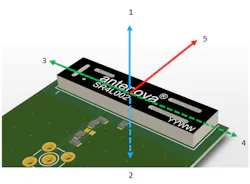
The corner of the PCB is generally the best place to position an antenna. That’s because a corner position allows the antenna to have clearance in five spatial directions, and the feed to the antenna lies in the sixth direction (Fig. 1).
Antenna manufacturers offer a choice of antenna designs that will be suited to different positions, so product designers can select the antenna that fits best into their layout, which are increasingly mixed-signal designs. Often, the manufacturer’s datasheet will show a reference design which, if followed, will deliver optimal performance.
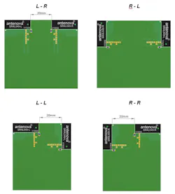
Product designs for 4G and LTE usually employ more than one antenna to build a MIMO system. In such designs, where multiple antennas are used simultaneously, the antennas are typically placed on separate corners of a PCB (Fig. 2).
How to Determine the Keep-Out Area of the Antenna
It’s important not to place any components in the near field immediately around the antenna, as they may interfere with its performance. Accordingly, the antenna specification will state the size of the keep-out area—this is an area near and around the antenna that must remain clear of metallic objects. This will apply to every layer in the PCB. In addition, no components, or even mounting screws, should be placed within this area on any of the layers of the board.
An antenna radiates against a ground plane, which is the part of a PCB design that provides a common reference point for electrical signals and serves as a return path for currents. The ground plane is related to the frequency at which the antenna operates. Thus, allowing the correct size and space for the chosen antenna’s ground plane is a top priority.
The Importance of Ground Planes to Antenna Placement
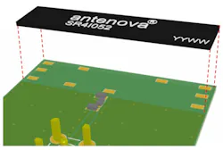
The ground-plane size should also consider any wires used for communication to the device and the batteries or power cable that power the device. If the ground plane is properly sized, it will ensure that the cables and batteries connected to the device have less influence on the antenna (Fig. 3).
Some antennas are ground-plane-dependent, which means that the PCB itself becomes the ground portion of the antenna to operate against in order to balance the antenna currents, and the lower layers of the PCB may affect the antenna’s performance. In these cases, it’s important not to place a battery or an LCD near the antenna.
The manufacturer’s datasheet should always specify whether the antenna needs a ground plane to radiate, and, if so, the size of ground plane required. This may mean that a clearance area should surround the antenna.
Keep Distance Between Embedded Antennas and Other Components
It’s vital to keep the antenna well away from other components that might interfere with the way the antenna radiates. Items to be wary of are batteries; LCDs; metal components such as USB, HDMI, and Ethernet connectors; and noisy or high-speed switching components related to switching power supplies.
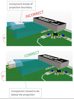
The ideal distance between the antenna and another component varies according to the height of that component. As a rule, if a line is drawn at an angle of 8 degrees from the base of the antenna, the component will be at a safe distance from the antenna if it’s positioned below this line. Figure 4 shows how this looks with a USB connector.
If other antennas are nearby operating on similar frequencies, the effect may be to detune the two antennas as they affect each other’s radiation. We recommend mitigating this by isolating the antennas by at least −10 dB up to 1 GHz and −20 dB for 20 GHz. This can be done by allowing more distance between the antennas or rotating them so that they are placed at 90 degrees or 180 degrees apart from each other.
Designing the RF Transmission Line to Embedded Antennas
The transmission line is the RF trace that carries the RF energy to and from the antenna to deliver the signal to the radio. The design for the transmission line needs to be 50 Ω, or it’s possible that it may reflect signals back to the radio and cause a degraded signal-to-noise ratio (SNR), which could possibly desense the radio receiver. The reflections are measured as voltage standing-wave ratio (VSWR). A good PCB design will exhibit a suitable VSWR measurement, which can be measured when the antenna is tested.
We recommend designing the transmission line with care. First, the transmission line should be straight, because if it has corners or bends, these can contribute to losses. It’s possible to minimize the noise and signal losses that can affect antenna performance by placing vias evenly along both sides of the trace, as these help to increase performance by isolating noise traveling along nearby traces or ground layers (Fig. 5).
Thinner transmission lines can be more lossy. RF matching components and the width of the transmission lines should be used to tune the antenna to operate at a characteristic impedance of 50 Ω. The dimensions of the transmission line can affect performance, and the transmission line should be as short as possible to allow the antenna to perform well.
A free tool to calculate grounded-coplanar-waveguide (GCPW) transmission lines can be found here: https://blog.antenova.com/rf-transmission-line-calculator
Use Impedance Matching to Improve Antenna Performance on a PCB
If you allowed for the correct ground plane and placed the antenna in the optimal position, you’ve made a good start, but more can be done to improve antenna performance. You can use a matching network to tune the antenna—this will compensate somewhat for any factors that might be affecting the antenna’s performance.
The key RF components are the antenna, its matching network, and its RF output. A configuration that places these elements in proximity will minimize signal losses. Similarly, if your design includes a matching network, the antenna will perform best if the trace length from the antenna matches that specified in the manufacturer’s product specification.
The exterior casing around the PCB may also make a difference. Antenna signals can’t travel through metal, so placing the antenna inside a metal case or a case with metallic properties will not be successful.
Likewise, be cautious about placing an antenna close to plastic surfaces, as this can be very detrimental to antenna performance. Some plastics such as glass-filled nylon are lossy and dampen the RF signal to the antenna. Plastic has a higher dielectric constant than air, which can affect signals severely. It means the antenna will register a higher dielectric constant, thus increasing the electrical length of the antenna and reducing the frequency at which the antenna radiates.
We suggest using high-quality FR4 circuit boards—they will be less likely to create any issues with RF performance.
About the Author
Geoff Schulteis
RF Antenna Application Specialist, Antenova
Geoff Schulteis is RF Antenna Application Specialist at Antenova. Geoff leads technical support for Antenova’s North American customer designs. He’s an antenna engineering professional with more than 20 years’ experience in designing, integrating, and testing antenna systems for consumer products from R&D through manufacturing and commercial deployment. Geoff is uniquely familiar with the wireless product development landscape, and he has designed antennas for various IoT applications using protocols ranging from 2G through 5G, earning him multiple patents.
Voice Your Opinion!
To join the conversation, and become an exclusive member of Electronic Design, create an account today!

Leaders relevant to this article:
