APUs vs FPGAs: The Battle for Smart-Camera Processing Supremacy
This file type includes high resolution graphics and schematics when applicable.
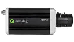
Innovation in smart-camera technology is accelerating quickly, yielding faster, smaller, and more power-efficient vision systems optimized for increasingly sophisticated tasks that can enhance productivity, precision, and security for a wide range of applications spanning industrial, scientific, surveillance, and beyond. This trend is particularly pronounced in the rapidly expanding domain of x86-based smart cameras (Fig. 1) that eschew conventional, narrowly supported FPGA processing platforms to enhance design flexibility, functional versatility, and rapid prototyping.
As competition in this market intensifies, design versatility becomes an increasingly critical metric for smart-camera vendors seeking to speed their time to revenue. It’s in this aspect, perhaps more than any other, that FPGAs show their age as a central processing element in modern vision systems. With FPGAs, product-development processes are impeded for even the most experienced design teams, and the learning curve for engineers honing their expertise in FPGAs is steep. Legacy FPGA-only-based smart cameras are sustained by designers with increasingly esoteric skill sets, which naturally impose limitations on development efficiencies.
FPGAs are complex, but high-performance, semiconductors that can be tailored for specialized target applications, and are compelling alternatives to x86 processors in some use cases. But their underlying value hinges mainly on the designer’s insight for defining internal hardware operations. On the software side of the equation, the competition for ease of development between FPGAs and comparably performing x86 processing platforms—particularly accelerated processing units (APUs)—isn’t even close.
We’d like to compare FPGAs with hard-CPU-core processing architectures to the more recent mass-market x86 APUs that combine GPU and CPU cores on a single die. In FPGAs with hard-CPU-core configurations, most vision-system applications require implementation of the more heavily computational image-processing algorithms in the FPGA fabric. It’s a rather significant limitation that requires the separate development of VHDL (VHSIC hardware description language), with its matching kernel drivers, for each target application. In this model, a simple change to an algorithm, data flow, or even debug and verification process requires a time-consuming re-spin of the FPGA implementation. A task partition model needs to be defined, with significant implications at the system level when “remodeling” is required.
In Qtechnology's implementation experience, the hard CPU core embedded on the FPGA was not powerful enough to inspect all of the data produced by the sensor in real time, so it was used merely to direct the flow of data. All of the imaging algorithms (image correction, segmentation, feature extraction, etc.) needed to be implemented in the fabric logic with VHDL.
Tipping the Scale
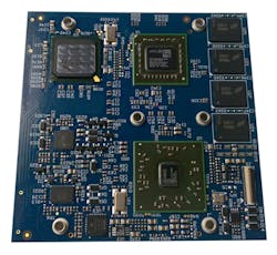
With x86 APUs (AMD Embedded G-Series T56N APUs, in our case) (Fig. 2), we can achieve previously unattainable development efficiencies. This is mainly due to the ability to tap open-source and third-party image-processing libraries such as OpenCV, Mathworks Matlab, and Halcon, as well as debugging tools for the onboard x86 CPU, and OpenCL for the GPU. Standard tools such as latency analyzers and profilers (perf, ftrace), modern debuggers and IDEs (Eclipse, gdb), power analyzers (powertop), and others can probe x86.
All of these tools are easily deployable with powerful build systems such as the Yocto Project, an open-source collaboration project that provides templates, tools, and methods to help users create custom Linux-based systems for embedded products regardless of the hardware architecture. Applications can be built and tested on any computer without the need of a custom cross-compiler or a poorly maintained board support package.
With an APU, a GPU combined onto the same die as the CPU enables the system to offload computation-intensive pixel data processing in the vision application from the CPU to the GPU without high-latency bus transactions. Freed from this task, the CPU can serve other interrupts with much lower latency, thereby dramatically improving the real-time performance of the entire system and better meeting the ever-rising processing demands of modern vision applications.
With this architecture, the whole processing platform can be governed by a standard Linux kernel, which requires only modest development support with each new kernel release. Board bring-up can be done on any OS (Linux, Windows), improving the time to market.
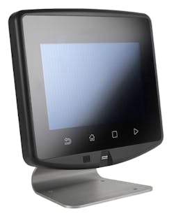
To further simplify and compress development cycles, we’ve integrated the APU into an industrial panel PC (Fig. 3) and I/O control module, giving us the ability to repurpose code across different systems via a single distribution based on the Yocto Project.
Adopting industrial standards, such as Ethercat and Modbus, often involves merely integrating already existent libraries. Since those libraries are usually developed under x86, there’s no need to port and maintain them.
One ancillary benefit of the AMD APU processing platform that we selected was the ability to scale up performance by pairing the APU with an AMD Radeon-based GPU in an MXM form-factor solution. This made it possible to harness additional processing resources to support a wider range of compute-intensive vision-system workloads when needed.
Open for Business
By using APUs rather than FPGAs as the central processing element in our smart cameras, we’ve gotten greater mileage from open development tools like OpenCL. This equips us and our customers to take full advantage of non-proprietary programming platforms to accelerate parallel processing performance, while scaling across a wide range of vision systems with a single source-code base. The ability to develop and maintain a future-proof, portable code base enables us to achieve significant programming efficiency gains and preserve the value of our core source code.
OpenCL, an open and royalty-free programming standard for maximizing parallel compute utilization on heterogeneous systems, gives vision-system designers a cross-platform, non-proprietary solution for accelerating their applications across mainstream processing platforms including APUs and multicore CPUs and GPUs. It provides a unified language to target all of the parallel-processing elements in use within a system. This is done by presenting the developer with an abstract platform model that conceptualizes all of these architectures in a similar way, as well as an execution model supporting data and task parallelism across heterogeneous architectures. OpenCL draws its syntax and workflow attributes from the software world, making it a much more accessible language than VHDL.
OpenCL can be implemented for FPGA-based smart cameras. But the ability to convert high-level programming languages to HDL for FPGAs still requires a fair amount of FPGA technology knowledge, and the market for OpenCL-to-HDL SDKs is sparse. Here again, the skill set required to effectively utilize FPGAs is highly specialized, the ecosystem of support tools is small, and development cycles are often protracted.
The Backbone’s Connected
Offering PC-caliber agility complemented by a robust ecosystem of industry-standard, x86- optimized software, x86 vision systems are unlocking multiple development, deployment, and management efficiencies. Among other capabilities, this allows our smart cameras to support neural networks that process real-time/high-frequency data into actionable information downstream on a factory floor in highly demanding markets.
Support for x86 also helps ensure tight integration with IT networks and x86-based distributed control systems, which introduces additional benefits for the applications hosted on these networks. We have easily implemented remote management and debug capabilities via the Internet, improving our customer service and enabling us to provide real-time data to clients for data-mining purposes.
Collectively, these efficiencies yield leaner cost structures for vendors, integrators, and end users alike, while overcoming the hardware/software incompatibilities and cumbersome software maintenance processes that have impeded FPGA-based vision system architectures.
This file type includes high resolution graphics and schematics when applicable.
Mind you, we don’t recommend abandoning the use of FPGAs in our smart cameras. Instead, we’ve traded our original FPGA-only processing architecture for an APU + low-cost FPGA architecture, partitioning the system in such a way that the low-cost FPGA only does the sensor interfacing and a fixed vision flow consisting of image preprocessing. This FPGA functionality is interfaced via Video4Linux2 (V4L2), the standard video-capture and output-device API and driver framework for Linux. Any standard application (Skype, Ekiga, etc.) or library (OpenCV, Gstreamer) can access the sensor. All other processing is done with standard computer vision libraries or user-defined OpenCL programs with no intervention from the hardware designers.
Advantages in Plain Sight
The shift away from specialized, legacy FPGA processing platforms and their limited ecosystem of supporting software is proving to be a tipping point for the vision-system industry.
Programmable, parallel-processing optimized APUs strike an ideal balance of x86 compatibility, performance, and scalability for a new generation of smart cameras, complemented by OpenCL- enabled acceleration and code portability.
About the Author
Kristian Madsen
Founder and Managing Director
Kristian Glöde Madsen founded and has served as managing director of Qtechnology since 2007. He previously spent more than 10 years in engineering and executive management roles via product development consulting engagements. He has participated in hundreds of electronic development projects.
Ricardo Ribalda
Firmware Engineer
Ricardo Ribalda, computer engineer (UAM, 2005) and MScRes in Computer Science and Telecom (UAM, 2007), is currently pursuing his Ph.D. He is a contributor to the Linux Kernel, U-boot, Yocto Project, and Flashrom. He is currently the firmware engineer at Qtechnology Denmark, where he’s helping to develop the next generation of industrial cameras.


