Implement Gate Drivers for 3-Level NPC2 Modules with Reverse-Blocking IGBTs
This file type includes high resolution graphics and schematics when applicable.
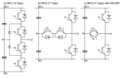
Three-level converter topologies can lead to reduced total harmonic distortion and, hence, minimize the size and cost of filtering at the output stage. However, the best-known configuration—Neutral Point Clamped (NPC1)—usually increases the required number of switching devices (IGBTs and diodes), which adds to the complexity of the system. However, a new topology, NPC2, based on reverse-blocking IGBTs makes it possible to reduce the power semiconductor count (Fig. 1).
Compared to the classical NPC1 setup (Fig. 1a), which consists of two IGBTs and four diodes in the clamping path, the NPC2 design in Figure 1b features a common collector topology. To reduce the amount of semiconductors in NPC2 setups, two reverse-blocking (RB) IGBTs can be used. RB-IGBTs can sustain forward- and reversed-biased voltages of equal levels, unlike standard IGBTs that can sustain only a fraction of the forward-blocking voltage when in reverse-blocking state. Therefore, with RB-IGBTs, NPC2 topology designs can be implemented using two fewer diodes (Fig. 1c). This offers several advantages, including reduced conduction losses, better utilization of package area, and simplified auxiliary terminal arrangement.
Gate-Driver Considerations
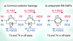
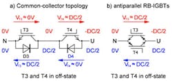
Common to all of the NPC topologies shown in Figure 1 is that during normal operation, the voltage of the phase output U alternates between 1/2 DC+ and 1/2 DC– with respect to the neutral point N. In other words, it changes its polarity. This is particularly significant for IGBTs between junctions N and U of the NPC2 topology that form the bidirectional switch. Figure 2 shows the resulting voltages for these IGBTs.
The collector-emitter voltage of the IGBT switches in Figure 2a is always positive or (idealized) zero, depending on the actual phase output voltage at position U. Hence, for short-circuit and overvoltage protection, no special requirements need to be considered. However, if RB-IGBTs are used, the alternating voltage at junction U will require modifications to be made to the short-circuit and overvoltage protection schemes. Otherwise, the gate-driver stage and eventually the power stage will be damaged.
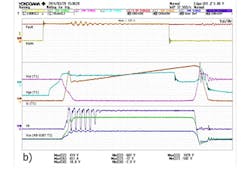
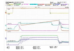
Figure 3 shows measurements using Fuji Electric’s NPC2 power module, model 4MBI300VG-120R-50. The load is connected between U and DC–, while the top switch, T1, is turned on and off. The waveform of channel 2 (Vce RB-IGBT T3) illustrates the alternating voltage between N-U during the turn-on and turn-off phases of IGBT T1.
Overvoltage Protection
To protect IGBTs against transient overvoltages during turn-off events, an active clamping circuit is commonly used. Active clamping reliably limits overvoltage by driving the IGBT into the active region and reducing the change of commutation current (di/dt).
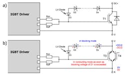
In a standard active clamping setup for IGBT T1 (Fig. 4a), transient-voltage-suppression (TVS) diodes (D2…Dx) are connected from the collector to the gate via a low-voltage Schottky diode or PIN diode (D1). This diode is necessary to avoid a current flow from the gate into the IGBT collector, and requires only a blocking capability of, for example, 40 V.
However, if an NPC2 topology with RB-IGBTs is selected, the typical active clamping circuit with unidirectional TVS diodes and a low-voltage diode cannot be used. That’s because the voltage across the RB-IGBTs will change the polarity depending on the switching states (Fig. 4b). As long as the polarity of the collector of the respective IGBT is positive, the corresponding gate driver’s TVS diodes can block this voltage from the driver. But as soon as the collector voltage reverses its polarity, the TVS diodes start to conduct and the full collector potential will be applied to the anode of the low-voltage diode D1. This voltage equals approximately half of the DC-link voltage, and would lead to the destruction of the IGBT and associated driver.
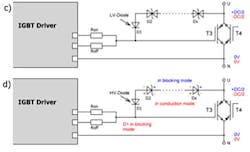
Two possible options can prevent this happening. The first uses a bidirectional TVS diode instead of a unidirectional device (Fig. 4c). However, as shown in Fig. 3, the negative voltage “Min (C2)” may reach levels that equal the break-down voltage of the bidirectional TVS diodes. If this occurs, diode D1’s reverse voltage will exceed limits. Consequently, this approach is not recommended.
The preferred solution replaces the low-voltage diode (D1) with a high-voltage device that has a blocking capability of at least half the DC-link voltage (Fig. 4d). Creepage and clearance distances of the diode package must also be considered, and it may be necessary to use more than one diode.
Short-Circuit Protection
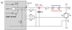
Protecting IGBTs of any topology during a short-circuit event requires a reliable desaturation monitoring function. Figure 5a shows a common implementation of desaturation monitoring with high-voltage diodes. If using an NPC2 topology with RB-IGBTs, though, the desaturation monitoring with high-voltage diodes method will no longer work. This approach is only effective when the corresponding collector voltage has positive potential (referenced to emitter) and the high voltage of the corresponding gate driver can block this voltage away from the driver’s low-voltage sense input. Once the polarity turns negative, the diodes start to conduct and an excessive current will flow through the diodes, which will damage the driver and/or associated IGBT.
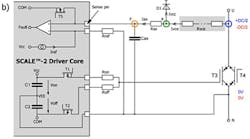
A more advanced solution is to replace the high-voltage diodes with a resistor network (RVCE in Fig. 5b). In this circuit, the VCE voltage is measured during the IGBT turn-on state, which avoids inadvertent tripping of the monitoring function. By implementing short-circuit protection using a resistor network, the RVCE resistors scale down the collector voltage and limit the current flowing from the collector to the gate-driver sense input.
Short-Circuit Protection with Resistor Network
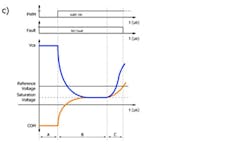
During an IGBT off-state, the driver’s internal MOSFET connects the sense pin to COM (negative potential of the gate driver) (Fig. 5b, again). The capacitor Cax is then pre-charged/discharged to the negative supply voltage. The function of D1 is to clamp the voltage VK to the positive supply voltage VCC to protect the gate driver’s sense input against high voltages. To limit the losses in the resistor network and diode D1, it’s recommended that the current at maximum DC-link voltage be adjusted to between 0.6 and 1 mA.
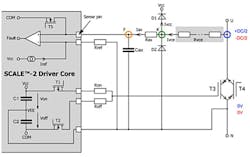
At IGBT turn-on and in the on state, the MOSFET turns off. While VCE decreases, Cax is charged from the COM potential to the IGBT saturation voltage. The voltage of Cax is continuously compared with a reference voltage determined by RREF. In the event of a short circuit, Cax voltage increases as the IGBT is driven out of saturation. Once the voltage of Cax is higher than the reference voltage, the gate driver will interpret this as a fault condition. Figure 5c illustrates this scenario.
If a negative voltage is present during the off state, the voltage at junction K will also be negative. To prevent a current flow out of the sense pin of the gate driver, another diode (D2) must be added (Fig. 6). Otherwise, substrate currents and unintended latch-up effects will occur within the gate-drive circuitry. (It’s also possible to implement active rectification inside the ASIC to address this point.)
The results of incorporating the additional diode D2 are shown in Figure 3b. When comparing channel 8 (VK) of both measurements, one can observe that the voltage VK is limited to a lower negative value (–2.9 V with D2 compared to –78 V without D2).
Conclusion
RB-IGBTs can be used in NPC2 topologies, bringing significant benefits to applications such as solar power and UPS systems, as long as attention is paid to the design of protection circuitry. Without these modifications, the gate driver and eventually the entire power stage will be damaged. That’s because the negative voltage at the phase output will overload the gate driver unit. These changes can be implemented using standard gate driver cores developed by Power Integrations.
This file type includes high resolution graphics and schematics when applicable.
Christoph Dustert is an engineer, System & Applications Engineering, and Andreas Volke is senior manager, System Engineering, for Power Integrations.
