Succinctly, a dc-dc converter is a power-supply device that does just that: Change a dc voltage to a higher or lower dc voltage. All electronic systems require constant voltage supplies to drive the signal-generating components and devices under their umbrella. Constant is a keyword because it’s possible to have a power converter that has a degree of ripple on the output voltage line. If you use a power converter with an output ripple, the challenge is to ensure that this ripple doesn’t interfere with the expected signal quality impacting the onboard chips.
The two fundamental types of dc-dc converters are linear and switcher. With the linear converter, the delivery of the source power is continuous to the load. The pass element for this continuous, linear signal to the load regulates the current flow between the source to the load. The other type of dc-dc power supply is a switcher converter. The switcher-type converter delivers bursts of power as the pass element is switching on and off.
Before we go any further, there are essential converter characteristics to keep in mind as you perform your final selection. The fundamental characteristics for your system requirements are in terms of the input-voltage range, output-voltage level, and current rating. But to dig a little deeper, knowing the efficiency and transient response of the dc-dc converter is equally critical. Finally, the size and cost of your application’s components may turn out to be the most critical specifications.
Linear Regulator
A low-dropout regulator (LDO) provides a stable dc output voltage for a stable dc input voltage. Usually, you find LDOs in radio-frequency and precise analog applications that have extremely small signal voltages. For these linear regulators, there’s no switching action, and consequently, electromagnetic interference (EMI) becomes a “no-worries” situation. The characteristics that these applications require from their power source are narrow VIN to VOUT differences, high precision, and low noise.
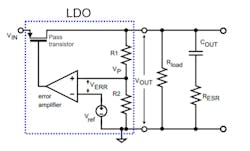
The fundamental construction of the LDO contains a current source, bandgap reference, amplifier, a pair of resistors, and a driving transistor (see figure).
Shown is a simplified LDO circuit.
In the figure, the input voltage (VIN) powers the pass transistor, voltage reference (VREF) and op amp. The op amp forces the non-inverting input to equal VREF, which in turn, from the R1/R2 voltage divider, establishes the voltage value at VOUT. The voltage reference in the LDO is usually a stable bandgap reference that provides a dc voltage at the inverting input of the op amp. The pass transistor provides the output drive current to the LOAD, while R1 and R2 hold VOUT steady.
LDOs have a fast transient response to accommodate the needs of FPGA or multicore processors, where fast changes occur in the load. The icing on the cake for LDOs is that they’re usually low cost and require fewer external components. There are no switching currents in or out of an inductor, which actually doesn’t exist in this circuit, minimizing the LDO’s EMI generation.
The efficiency of any power device is equal to:
Efficiency = POUT/PIN
where POUT is equal to the power out or VOUT x IOUT, and PIN is equal to the power in or VIN x IIN.
Looking at the figure, the VIN must be greater than the VOUT + VPass transistor. This relationship locks in the efficiency of the LDO. Basically, the IOUT value tracks the IIN value. In addition, if VIN is much greater than VOUT (which is independent of IOUT and IIN), the efficiency becomes worse. In many circuits, this efficiency disadvantage of the LDO can eliminate it as an option. From there, the only alternative is to use a switching power supply, if you can tolerate the output switching noise.
Which brings us to this column’s next installment. In a few weeks, you will see the inner workings of inductive switching supplies.
About the Author
Voice Your Opinion!
To join the conversation, and become an exclusive member of Electronic Design, create an account today!

Leaders relevant to this article:


