What’s the Difference Between CMOS Switches and Solid-State Relays?
Members can download this article in PDF format.
What you'll learn:
- How to derive off capacitance between the source and drain from off isolation.
- Comparisons drawn between CMOS switches and solid-state relays.
- Advantages of using CMOS switches.
Off capacitance between the source and drain (CDS(OFF)) is a measure of an off switch’s ability to block a signal on the source from coupling to the drain. It’s a common specification seen in solid-state relays (also known as PhotoMOS, OptoMOS, photorelays, or MOSFET relays), and is often referred to as output capacitance (COUT) in solid-state relay datasheets.
CMOS switches don’t usually include this specification. However, the off-isolation spec is a different method to characterize the same phenomenon—i.e., the amount of a signal presented to the source of an off switch that couples to the drain.
This article will discuss how to derive CDS(OFF) from off isolation and how this can be used to compare the performance of solid-state relays and CMOS switches more effectively. This is important as CMOS switches are a fit for many applications where solid-state relays are used, such as switching dc and high-speed ac signals.
How to Derive CDS(OFF) from Off Isolation
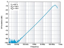
Figure 1 shows the off isolation vs. frequency typical performance plot of the ADG5412. The plot shows that as the frequency of the signal on the source increases, the off isolation decreases.
1. ADG5412 off isolation vs. frequency, ±15-V dual supply.
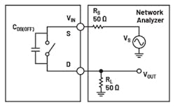
This means that more of the signal present on the source will appear on the drain of an off switch as the signal’s frequency increases. This isn’t surprising when you investigate the equivalent circuit for a switch in the off condition, as shown by the test circuit in Figure 2.
2. This is an off-isolation measurement test circuit.
When a switch is open, there’s a parasitic capacitance between source and drain, shown as CDS(OFF) in Figure 2. This parasitic capacitance enables high-frequency signals to pass, and to characterize this is the purpose of the off-isolation plot.
Off isolation is calculated by taking VS and VOUT from the Figure 2 test circuit and inserting them into the following equation:
Using the results of the off-isolation plot combined with the equivalent circuit of an open switch, CDS(OFF) can be calculated in a CMOS switch. First, if we consider the off-switch channel and the load, we can equivalate the circuit to a high-pass filter (Fig. 3).
3. Shown is CDS(OFF) and an RL high-pass filter.
The transfer function of the circuit shown can then by derived by:
Next is to consider the source voltage (VS) and its impedance from Figure 2. The source impedance (RS) is 50 Ω and this matches the load impedance (RL) of 50 Ω. If we assume the ideal case where CDS(OFF) is a short circuit, then VS is double VIN, as the impedances are equal. Thus, when the transfer function is calculated in relation to VS, the overall transfer function is doubled.
Therefore, the transfer function of the whole system is:
This transfer function can then be substituted into the off-isolation equation to give:
This equation can then be rearranged to make CDS(OFF) the subject:
Therefore, if we know RL, the frequency of the input signal (f), and the off-isolation specification value in dB, the CDS(OFF) can be calculated. These values are typically found in the datasheet of switch or multiplexer products in the Analog Devices portfolio. The following example will outline how it can be done.
Calculation Example CDS(OFF)
The ADGS1612 SPI-controlled, quad SPST switch will be used in this example. The off-isolation specification of the ADGS1612 is −65 dB, and this can be read from Table 1 of the datasheet. From the test conditions section of the off-isolation specification, RL is given as 50 Ω and the signal frequency (f) is stated as 100 kHz. By putting these values into the CDS(OFF) equation, the capacitance value can be calculated:
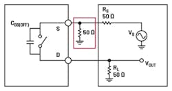
Note, the measurement circuit for off isolation for switches and multiplexers may contain an additional 50-Ω termination before the source pin of the switch channel (Fig. 4). The CDS(OFF) equation can still be used with off-isolation specifications that were measured in this way.
4. Off-isolation test circuit with a 50-Ω termination on the source.
However, 6 dB must be added to the off-isolation specification from the datasheet when a 50-Ω termination is used at the source pin before using it in the CDS(OFF) equation. This is to compensate for the fact that the 50-Ω termination at the source decreases the voltage by half, which is equivalent to −6 dB.
CMOS Switches vs. Solid-State Relays
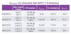
The table shows the CDS(OFF) values for a selection of Analog Devices switch products. The ADG54xx and ADG52xx families can handle signal voltages with up to a 44-V swing, while the ADG14xx and ADG12xx families can pass signal voltages with up to a 33-V swing. This comparable signal ranges to 30- and 40-V solid-state relays.
The last column in the table also shows how the CDS(OFF) can be used in conjunction with the switch on-resistance to calculate the RON, CDS(OFF) product, which is used as an order of merit in solid-state relays. The RON, CDS(OFF) product indicates how little a switch will attenuate a signal when it’s on, combined with how well a switch can block high-speed signals when the switch is off. The table shows that the ADG1412 has an RON, COFF product of less than 5, which is extremely competitive to comparable solid-state relays.
There are also many advantages of CMOS switches compared to solid-state relays. These include:
Easier to drive switch logic: The typical digital input current for most Analog Devices CMOS switches is 1 nA, while the recommended forward current for the diode in solid-state relays is 5 mA. This means that CMOS switches can be easily controlled directly by the GPIOs on microcontrollers.
Faster switching speeds: The ADG1412 has a typical turn-on time of 100 ns compared to solid-state relays, which have turn-on times in the region of hundreds of milliseconds.
More switches per package: For example, the ADGS1414D has eight switch channels with 1.5 Ω on-resistance and 5-pF CDS(OFF) in a 5- × 4-mm package. That’s one switch per 2.5 mm2 of package area.
Conclusion
The ability of a switch to block signals when in the off state is key. In solid-state relays, the COFF specification is a measure of the capacitance across the switch, which allows the coupling of signals from the input to the output of the closed switch. In CMOS switches, this capacitor isn’t directly measured. However, the effect of this capacitor is measured through the off-isolation specification.
The off-isolation value in dB, the frequency of the input signal, and the load resistance can be used to determine the CDS(OFF) by deriving the transfer function of an open switch. The CDS(OFF) is important in comparing CMOS switches to the COUT specification of solid-state relays.
Furthermore, CDS(OFF) also can be used to calculate the RON, CDS(OFF) product, which is an order of merit that’s used to show the overall off isolation and signal-lost performance of a switch. This allows for direct competition between CMOS switches and solid-state relays when selecting a switch for an application.
CMOS switches also have many benefits over solid-state relays—namely, easier to drive switch logic, faster switching speeds, and the ability to have more switches in a package.


