Performing Key Switch-Mode Power Supply Measurements on an Oscilloscope
For some applications such as extremely low-noise amplifiers or precision automated test equipment, it’s still possible to find a linear power supply at work converting AC utility power into some form of DC power. If having output that is virtually free of noise or ripple is the top priority, designers are willing to put up with a linear power supply’s 20% to 40% power efficiency and large size and weight. But for nearly everything else, switch-mode power supplies (SMPS) have become the dominant architecture for converting power from either AC or DC to one or more DC levels.
In contrast to a linear power supply, an SMPS offers major advantages in efficiency (85-90%), size, weight, precision, and flexibility. They also tend to generate less heat and have better regulation under a variety of changing loads. Because of these advantages, SMPSs are found in an extensive range of applications spanning nearly all digital products like computers and mobile device chargers, automotive charging, medical equipment, audio equipment and even industrial equipment such as arc welders.
That said, there is no such thing as a free ride, and SMPS designers have a variety of challenges they must grapple with. These include greater complexity, the generation of high-amplitude, high-frequency energy that a low-pass filter must block to avoid electromagnetic interference (EMI), and ripple voltage at the switching frequency, as well as at the associated harmonic frequencies.
Ideally, every power supply would behave like the mathematical models used to design it. But in the real world, components are imperfect, loads vary, line power may be distorted, or environmental changes can alter performance. The list goes on. And designers are expected to create a power supply that takes up less space, is more efficient, reduces heat, cuts manufacturing costs, and meets tougher EMI/EMC standards.
Making the right design choices requires careful characterization and troubleshooting of the design. Fortunately, these tasks can now be performed easier than ever using a modern oscilloscope coupled with automated power analysis software that does much of the heavy lifting.
SMPS measurements
Let's start by looking at the simplified SMPS schematic in Figure 1. The power signal path of a typical SMPS includes passive, active, and magnetic components. To maximize efficiency, SMPS designs minimize the use of lossy components such as resistors and linear-mode transistors, and emphasize components that are (ideally) lossless: switch-mode transistors, capacitors, and magnetics.
SMPS devices also include a control section containing elements such as pulse-width-modulated regulators, pulse rate-modulated regulators, and feedback loops. Control sections may have their own power supplies. SMPS technology rests on power semiconductor switching devices such as MOSFETs and IGBTs. These devices offer fast switching times and are able to withstand erratic voltage spikes.
The most important measurements that need to be performed on an SMPS are captured in Figure 2 and involve the input filter, switching device and the rectifier and filter. Using a modern oscilloscope with integrated power measurement and analysis software simplifies setup and makes it easier to conduct measurements over time. To be sure, careful probing and optimization also important factors in making sure you get good results.
Output ripple
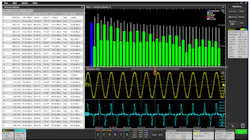
The first measurement we'll look at is the output voltage ripple on the power supplies output or load. The definition of ripple is simply the AC voltage that is superimposed onto the DC output of a power supply. Linear power supplies usually see a ripple that is close to twice the line frequency, whereas switch mode power supplies may see switching ripple in the hundreds of kHz. As shown in Figure 3, automated oscilloscope measurements for ripple removes the DC components on output voltage waveform and calculates the RMS, and peak to peak values for the remaining AC components.
Ripple measurements can focus on either the line related components or the frequency of the switching device itself. As shown in Figure 3 we're measuring the switching ripple, and the automated ripple measurements appear in the results badge on the right side of the display screenshot. Other additional standard oscilloscope measurement tools can be used to further investigate and analyze the ripple as well. In the upper portion of the display, cursors are used to measure the frequency content of the signal in the frequency domain. Meanwhile, in the lower part of this display you can get a visualization of switching ripple in the time domain. Together, these measurements provide comprehensive characterization of the amount of ripple a particular SMPS design is producing.
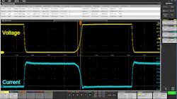
For switching device measurement, a differential probe is used to measure the voltage across the switching device and then a current probe is used to measure the current of the switching device. With this set up in place, one of the first measurements you’ll want to take a look at is slew rate, or the rate of change of both voltage and current when the switching transistor turns on and off. In Figure 4, the power analysis software on the scope has made over 1,000 acquisitions and accumulated enough “rich data” to deliver the results shown. In this case, you can see that the switching device turns on much faster than it turns off.
Power & switching loss
In most switching power supplies, losses primarily occur when the device is switching between on and off states. Turn on loss happens when the switching device changes from its non-conducting state to its conducting state. Conduction losses are when the switching device is in saturation. Turn off loss is the energy losses when the switching device changes from its conducted state to non-conducted state.
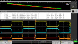
In Figure 5, the total switch loss measurements are shown in the results badge on the right side of the display. The power application analyzes the signals and defines the specific measurement regions. In this case, the turn on region begins when the voltage and current rise to 5% of amplitude, and ends when both fall to 5% of amplitude. The conduction region then is located between the turn on and turn off regions, and the total switching loss is simply the sum of the losses.
The trajectory plot at the top of the display in Figure 5 offers a handy x-y display of voltage versus current during the turn on state in green and the turn off state in red. In this particular case, you can see that the current varies fairly linearly with the voltage.
Another common measurement performed on a switching device is safe operating area mask testing. A switching device may fail if the maximum instantaneous current, maximum instantaneous voltage or maximum instantaneous power are exceeded. Particularly for today’s higher powered devices, understanding SOA has become much more critical. It is often useful to evaluate the SOA plot for the diverse operating conditions a power supply may encounter.
To characterize the operating region, the SOA measurement plots of voltage versus current provide a simple, visual way to see if a device remains within specified limits. In Figure 6, the gray mask represents the disallowed operating area for the device. In this example, the maximum specs for the switching device are used to define the mask: 45 A maximum current to the switching device, 60 V maximum voltage and 125 W maximum of instantaneous power dissipation in the switch device. Here, the switching device is well within the maximum specifications.
Modulation analysis & power quality
Modulation operation can be analyzed at power on during normal operations with changing line voltage conditions and also with changing loads. Modulation analysis is useful for characterizing the pulse-width modulation feedback from the DC output to the switching transistor’s gate terminal for dynamic voltage regulation. It also can provide insight about the turn-on characteristics of a switching power supply.
In the screen shot in Figure 7, the yellow voltage waveform is the FET gate driver control signal at power on, the green waveform shows the time trend of the positive pulse width modulation measurements, and the red waveform shows the time trend of the negative pulse width modulation measurements. The measurement results are accumulated at the top of the display and allow you to verify that the control signal remains within design specs during the power up phase.
Power line measurements characterize the interaction of the supply and its service environment. It is good to remember that power supplies can be of any size, from the small fan feed boxes inside a personal computer, to the sizeable devices supplying factory motors, to the massive supplies supporting phone banks and server farms. Each of these has some effect on the incoming power source (typically utility power) that feeds it.
To determine the effect of the insertion of the power supply, power voltage and current parameters must be measured directly on the input power line. Power quality does not depend on the electricity producer alone. It also depends on the design and manufacture of the power supply and on the end-user’s load. The power quality characteristics at the power supply define the “health” of the power supply. To determine the power consumption and distortion on the power line, power quality measurements are made at the input stage
As shown in Figure 8, automated power quality measurements provide a quick comprehensive table of measurement stats for the AC input section of a power supply conversion circuit. The measurements essentially include everything you would want, including line frequency, RMS voltage and current, voltage and current crest factors, true power, reactive and apparent power while adding power factoring and phase angle. In this example, the orange math waveform shows the instantaneous power. while the purple waveform shows the instantaneous energy in the acquisition.
Harmonics analysis/Total harmonic distortion
Current harmonic measurements are another important indicator of power quality and are often required for many standards to avoid disturbance to other equipment connect to the AC supply. The main measure is total harmonic distortion or THD, the cumulative value of distortion contained in the harmonics of the fundamental line frequency. As shown in Figure 9, measurements can be made on the first 40 harmonics up to a total of 100 harmonics.
This is particularly important with higher frequency power supplies where harmonics can be more of a problem. In addition to amplitude measurements, the harmonics results table at the left side of this screenshot shows the frequency magnitude and phase measurements on each harmonic. This visualization also provides a tool for evaluating margin compared to standards, indicated by the white line overlaid on the results chart.
Conclusion
Power supplies are integral to virtually every type of electronic products in use today and SMPS has become the dominant architecture for the majority of these products, offering greater efficiency and smaller weight and size, but with more complexity. To bring SMPS designs to market, complex measurements are needed for verification of reliable product operations and for regulatory compliance testing. To meet the demand, repeatable automated power measurements on an oscilloscope are key to ensuring that your designs are reliable, safe and compliant.
About the Author
Wilson Lee
Technical Marketing Manager
Wilson has over 25 years of technical marketing, technical sales leadership roles with manufacturers such as CTS Electronic Components, as well technical/value-add distributors such as Richardson RFPD and Premier Farnell. Wilson has focused heavily on design and design engineer engagement within the RF/wireless, industrial power, and industrial automation market segments.
Wilson earned his Bachelor’s of Science at Cornell University. He has lived in New York, Chicago, and Asia through his career, and currently resides in Portland, Oregon.
Voice Your Opinion!
To join the conversation, and become an exclusive member of Electronic Design, create an account today!

Leaders relevant to this article:


