“Probing” the Future of Power Integrity Test and Measurement
What you'll learn:
- Voltage regulator modules and power-distribution-network impedance.
- Methods for measuring PDN impedance.
- Overcoming a probe's high ground loop resistance with a low-noise isolator.
Power integrity (PI) is all about delivering the appropriate power from the voltage regulator module (VRM) to the load to maintain proper and reliable operation under dynamic loading conditions. As a result, design margins that allow for reliable product performance must be considered and maintained.
Next-generation ASIC power-delivery requirements continue to rise, and they show no signs of stopping. This means the target impedances of power distribution networks (PDNs) continue to decrease to even lower levels, into ultra-low impedance territory (sub-100 μΩ).
PDN impedance is determined by the VRM and its associated output capacitance, power paths through the printed circuit board (PCB), decoupling capacitance, and loading. All of these factors impact the impedance of the pathways in the design.
The key challenge for engineers grappling with PI is that the dynamic load can operate from DC to GHz, resulting in extreme bandwidths. The impedance requirement of the power path, often referred to as the “target impedance,” is an effective tool for designing power delivery over the full bandwidth. However, its variations may cause load step noise that can violate the recommended power-supply voltage of downstream ICs, as well as trigger other problems.
Given normal component variations and tolerances, and several unknowns, the target impedance can have wide variances. Nonetheless, it can be simulated—or even better—measured.
A More Advanced Probe for Power-Integrity Testing
The PDN (Fig. 1) contains important impedance information that can tell a designer how a system will react to dynamic currents. But figuring out the impedance can be a daunting task by itself. A voltage regulator’s output impedance isn’t typically available from component vendors—and not always accurate when it is. Furthermore, measuring ultra-low impedance on multiple VRMs or a multi-topology VRM is a challenge for any design engineer.
The 2-port shunt-thru measurement is the gold standard for measuring output impedance in the sub-milliohm region. However, it can be a challenging measurement. It’s not always possible to make these measurements unless engineers have direct SMA connections to the PCB.
When these types of measurements are made with a VNA, care must be taken when connecting the device under test (DUT) to ensure inductance is minimized, allowing for accurate measurements. Problems in the PDN are significant and costly. They can often require a board spin to fix.
In the past, performing PDN impedance measurements required soldering of coax or preparing the PCB with RF connectors for measurement or the use of a pair of single-port probes.
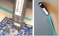
Another way to approach the problem is with the Picotest P2102A probe (Fig. 2). The P2102A is a 50-Ω transmission-line, 4-point Kelvin probe with many use cases, one of which is PDN impedance measurement with the 2-port shunt-thru methodology. One of the advantages of the probe is that the pogo pins allow for solderless probing in dense areas without the need for test points. The rugged design and small form factor also make it possible to get into tight places.
The P2102A is referred to as a “browser” probe for its ability to quickly be moved from point-to-point and rail-to-rail simply by reseating the probe points. The probe achieves low inductance at the tip to mitigate space constraints on a high-density PCB.
At the same time, the probe eliminates the need to add additional SMA connections or other test points necessary for impedance measurements. It’s particularly useful when multiple rails must be tested, and repeated measurements are simplified because connection is by simply touching the tip to existing output capacitor pads.
But these advantages can also pose problems, including the fact that they could complicate ultra-low impedance measurement. Two major obstacles emerge when it comes to measuring very low impedance—noise and ground loop error.1 The ground loop error can be reduced by minimizing the shield resistance in the cables used in the measurement setup and/or increasing the common-mode rejection ratio (CMRR). In this case, the probe GND pin tip resistance introduces a significant unavoidable (and variable) ground loop error in the measurement.
This raises a couple of questions. First, what exactly is the probe GND pin tip resistance? Second, can the ground loop error be reduced enough to make the P2102A capable of measuring ultra-low impedances?
Probing the Problems with Ultra-Low Impedance Test
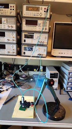
Following the measurement flow in Figure 3, the first step is to figure out how to calibrate the setup. As previously noted, the measurement technique is the 2-port shunt-thru method. The calibration method that worked effectively in this case was MEAS-SHORT, in which an ideal short is used to measure ZERO and, thus, null out any fixture effects.
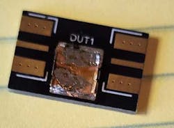
The ideal short in this case was a 60-oz. copper slug (previously a penny was used) placed on the PCB (Fig. 3). Applying a Kelvin sense measurement, it came out to a relatively minute 1.2 μΩ.
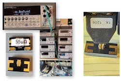
Once calibration is complete, it’s necessary to create a known DUT (Fig. 4). The DUT was nominally 55 μΩ, but its actual measured resistance came out slightly higher at 60 μΩ.
Next comes quantifying the probe GND pin tip resistance. To do so, one must measure the SHORT, but not with Kelvin sense. Instead, it made more sense to measure the voltage between the second probe’s SIG to the first probe’s GND (Fig. 5). This measurement included a one-meter coax cable, with a GND shield resistance of 14 mΩ. The total measured resistance came out to 26 mΩ. Therefore, the measured probe GND pin tip resistance is 12 mΩ.
However, it’s important to note that the pins were depressed in this measurement. More pin pressure reduces the resistance slightly, so a more conservative estimate of the probe GND pin tip resistance is 20 mΩ. This means the total ground loop resistance equals 34 mΩ:
There’s nothing to do to reduce this ground loop resistance. So, another possibility is to reduce the CMRR:
But how much CMRR is required?
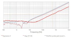
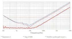
The challenge is that 82-dB CMRR is already a tall order. On top of that, the CMRR needs to be 82 dB at low frequencies to accurately measure the PDN DC impedance, which must remain under 100 µΩ. The Picotest J2113A differential amplifier is 25 dB below this requirement. The J2102B common-mode transformer can get close but only in the mid-kHz range.
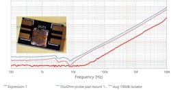
However, a prototype isolator currently in development by Picotest may fit the bill. It’s not broadband like the J2102B, but it has 100-dB CMRR at low frequencies and is very low noise.
All three isolators (J2113A, J2102B, and the 100-dB prototype) were used to measure the 60-µΩ DUT. To reiterate, the measurement method was 2-port shunt-thru using the P2102A probe, and the calibration method was MEAS-SHORT (Fig. 6). What follows are the results.
The J2113A isolator fails to accurately measure the DUT at low frequencies due to its limited CMRR (Fig. 7).
Conversely, the J2102B isolator does a better job than the J2113A. Above 1 kHz, the measured value is fairly accurate. Below 1 kHz, it’s somewhat accurate but is noisy (Fig. 8).
The prototype 100-dB isolator performs the best out of all of them. The measurement is accurate and noise-free at low frequencies. This is a successful measurement (Fig. 9).
Ultra-Low Impedance Test: Possibilities for the Future
While Picotest’s P2102A probe can measure ultra-low impedances in the sub-100-µΩ range, it faces limitations. But the high ground loop resistance of the probe can be overcome using a very-high-CMRR low-noise isolator in conjunction with an ideal SHORT.
Employing either a separate amplifier to boost the signal-to-noise ratio (SNR) or a vector network analyzer (VNA) with a higher dynamic range could help improve the measurement even further. A possible next step is to explore different calibration methods, which ultimately may be more accurate due to vector error correction (starting with response-thru calibration and ending with full 2-port SOLT calibration).
References
1. Steve Sandler, Jeffrey Miller, Jason Sekanina, Heidi Barnes, Ben Dannon, “The Impact of Data Center & AI Growth on SI/PI Engineers,” DesignCon 2024.
2. S. M. Sandler, “How to measure ultra-low impedance (100uOhm and lower) PDNs,” EDI CON, October 2018.
3. S. M. Sandler, “The Simple Truth about Complex Impedance Probes,” 11th Power Analysis & Design Symposium, March 9, 2022.
4. S. M. Sandler, “Cable Shield Resistance Issue in a 2-port Impedance Measurement,” Signal Integrity Journal, November 15, 2021.
5. Benjamin Dannan and Steve Sandler, “Calibrating the 2-Port Probe for Low Impedance PDN Measurements,” Signal Integrity Journal, May 18, 2021.
6. Benjamin Dannan and Steve Sandler, “The Challenge of Measuring a 40 µΩ, 2000 Amp PDN With a 2-Port Probe: The Measurement Result,” Signal Integrity Journal, January 4, 2024.
About the Author
Rohan Phadke
Signal and Power Integrity (SI/PI) Engineer, Arista Networks
Rohan Phadke is a Signal and Power Integrity (SI/PI) Engineer at Arista Networks, where he works on developing high-frequency measurement methods and devices for high-performance network switches. He has previously worked at Keysight Technologies on the 70-GHz PNA product family. He received his MSEE from Stanford University.
Steve Sandler
Steve Sandler is the founder and chief engineer of AEi Systems LLC and the president of Picotest. At Picotest he is responsible for signal injector product development, as well as the overall operation of the test equipment company.
Charles Hymowitz
Managing Director, Chair, and CEO
Charles E. Hymowitz, managing director, is chair and CEO of AEi Systems LLC. Also, he was a cofounder of Intusoft and SalesMountain. He was the co-author and editor of SPICE Circuit Handbook, Simulating with SPICE, The SPICE Cookbook, Power Specialist’s App Note Book, and The SPICE Applications Handbook. He is a graduate of Rutgers University with a BS in electrical engineering as well as the Stanford University Executive Institute program for Management of High-Technology Companies. He can be reached at [email protected].


