Download the PDF version of this article.
Efficiency is an important dc-dc converter characteristic, particularly for virtually every battery-based or embedded system. It impacts the thermal and electrical losses in the system, as well as the cooling required. Also, it affects the physical package sizes of both the power supply and the entire system. Plus, it has a direct effect on the system’s operating temperatures and reliability. These factors contribute to the total system cost, both in hardware and field support.
Battery-based dc-dc converter efficiency determines battery life and run time. These converters must be small and lightweight as well as efficient, so they usually employ analog techniques. This will probably continue because of size and cost limitations. Most handheld battery-based systems have a built-in dc-dc converter integrated with other circuits (see “DC-DC Converter Systems Glossary”).
The Texas Instruments TPS8267x is a complete dc-dc converter for low-power applications. Housed in a compact, low-profile ball-grid array (BGA) package, it suits automated assembly. Its IC-like package includes the switching regulator, inductor, and I/O capacitors, so it doesn’t require any additional components.
The TPS8267x is a synchronous, step-down converter that works with a 2.3- to 4.8-V input. Operating at 5.5 MHz, it can provide up to 600-mA output and has good load and line-transient response. Its ~17-µA quiescent current helps maintain high efficiency at light load while preserving a fast transient response for applications that require tight output regulation.
If the load current decreases, the converter automatically enters a power-save mode where it operates in discontinuous current (DCM), single-pulse pulse-frequency-modulation (PFM) mode. The converter exits the PFM mode and enters pulse-width-modulation (PWM) mode when the output current can no longer be supported in PFM mode. As a result, the dc output voltage is typically positioned approximately 0.5% above the nominal output voltage. There's a seamless transition between PFM and PWM.
Digitally Based Design
Digital control is now appearing in embedded systems to augment or supplant analog techniques. Point-of-load (POL) converters in embedded systems are among the first to incorporate digital technology. Because embedded systems usually use several POLs, they have been good candidates for efficiency optimization.
GE Power’s DLynx Distributed-power Open Standards Alliance (DOSA) modules are digitally oriented POLs. The modules require only three external components and offer double the density of a discrete power design. Their standards-based DOSA footprints and analog/digital compatibility with existing circuit board designs shrinks the size, lowers the cost, and improves the performance of dc-dc converters.
Digital control provides the ability to monitor load power consumption. The DLynx modules deliver optimized current derating and 96% efficiency. Also, adaptive voltage scaling (AVS) leverages silicon performance to reduce power consumption through tight digital control (±0.4%) of the output voltage and a ±1% controller setpoint reference.
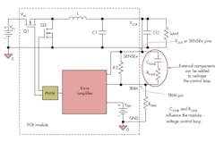
These modules include Tunable Loop technology that improves the converter’s transient response by modifying the POL’s control bandwidth. As the control bandwidth increases, the transient response improves for a fixed external capacitance. Increasing the control bandwidth and external capacitance together would improve transient response.
However, these parameters are interdependent. Increasing the external capacitance degrades the system’s control bandwidth. With the Tunable Loop, the control loop can be retuned to compensate for the additional external capacitance, which yields the best possible transient response.
The Tunable Loop employs an external network consisting of a resistor and capacitor in series connected across the TRIM and VOUT (or SENSE) pins of the POL module (Fig. 1). These networks use resistors of up to a few kilohms and capacitors from a few hundred picofarads to a few hundred nanofarads. This allows a single POL module to be externally optimized across multiple applications of significantly varying demands and yields the optimum board area, cost, response, and reliability.
Transients and surges applied to system power supplies can affect associated loads and cause system and component failure. To combat this, Linear Technology’s LTC4366 “surge stopper” IC interfaces between a system power supply and its loads, protecting the loads from the supply’s input-voltage surges.
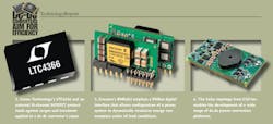
The LTC4366 protects loads by controlling the gate of an external N-channel MOSFET to absorb the surge (Fig. 2). Normally, the IC and MOSFET allow the power supply to service its loads with minimal insertion loss. But if the power-supply input receives a surge or transient, the LTC4366 and MOSFET clamp the voltage applied to the loads to protect them from damage or failure.
A floating topology allows the LTC4366 to operate from inputs of 9 V to more than 500 V. Its adjustable, regulated output clamp voltage does not affect system operation.
The Ericsson Power Modules 3E series BMR462 converter also uses digital control to offer a wide range of monitoring functions (Fig. 3). It operates with a 4.5- to 14-V input and produces an output from 0.6 to 5 V. At half-load, 5 VIN and 3.3 VOUT, typical efficiency is 97.1%.
A PMBus command can automatically control power dissipation under light-load conditions, minimizing current drain and switching losses. At low load currents, the BMR462 turns off its low-side MOSFET gate drive in its synchronous rectifier output, which boosts efficiency.
Isolated POL
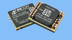
In a departure from most conventional non-isolated POLs, Vicor’s Picor Division developed the PI3106, an isolated POL converter with a high-efficiency, soft-switching power architecture. This topology allows the PI3106 to operate in distributed power architectures without requiring isolated power inputs (Fig. 4).
The PI3106’s 16- to 50-V dc input range and 334-W/in.3 power density enable it to deliver ~50 W (12 VOUT at 4.2 A). Housed in a space-saving 0.87- by 0.65- by 0.265-in. surface-mount (SMT) package, it reduces space by about 50% compared to traditional converter topologies.
A 900-kHz switching frequency allows the PI3106 to use small input and output filter components, further reducing the total system size and cost. Its output voltage is sensed and fed back to an internal controller using a proprietary isolated magnetic feedback scheme that allows high bandwidth and good common-mode noise immunity. It requires no external feedback compensation.
The PI3106 feature set includes output-voltage trim capability, output overvoltage protection, adjustable soft-start, overcurrent protection with auto-restart, and over and under input-voltage lockout. Also, its temperature monitoring and protection function provides an analog voltage proportional to the die temperature as shutdown and alarm capabilities.
Another type of dc-dc converter developed by CUI Inc. employs the Solus Power Topology, which combines a single-ended primary-inductor converter (SEPIC) with a buck converter to form a SEPIC-fed buck converter. Increased efficiency is accomplished by reducing both the conduction and switching losses at several critical points within the converter circuit.
The loss reduction is so significant that it can increase the output current by 40% for a given power-supply package size. Conversely, the loss reduction enables increased efficiency by several percent for a given output current and package size compared to the traditional buck topology.
The Solus topology includes one magnetic component, one control switch, and two commutation switches that are optimally PWM-controlled. The magnetic component consists of four inductively coupled inductors wound on the same core. This translates to a level simplicity on par with a traditional buck converter.
Also, Solus reduces I2R losses by channeling the operating currents into multiple paths. When the input current enters the converter, the topology branches that input into multiple paths, with each path carrying a lower current. This reduces conduction losses to a level that's significantly less than the losses within a standard buck converter.
Multi-current paths also reduce the voltage stresses on components by nearly 50%. With lower applied currents and voltages, the Solus topology reduces high-side MOSFET turn-on losses by better than 75% compared to the traditional buck.
The first product based on the Solus topology is CUI’s NQB series isolated dc-dc quarter brick (Fig. 5). This 720-W intermediate bus converter will initially support an input range of 36 to 60 V with a 12-V output and efficiency greater than 96%.
Brick Converters
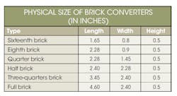
Brick converters are a defined physical size, but their efficiency can depend on whether power MOSFETs, gallium-nitride (GaN) transistors, or silicon-carbide (SiC) transistors are in the output stage (see table). All eighth bricks will have very similar maximum power-loss numbers, between 12 and 14 W, at full power as the amount of heat that can be removed from the module is purely size-dependent.
A typical eighth-brick converter that's 90% efficient at full load will have a maximum output power of no more than 125 W (assuming 14-W loss). Improving the efficiency by just 2% increases the available output power to 160 W, a 28% improvement.
It’s possible to reduce the power loss in the magnetic components (up to a point) by increasing their operating frequency. However, this isn’t normally done because the increase in frequency-dependent semiconductor losses outweighs that potential improvement. Usually, the operating frequency is reduced to maximize the magnetic structure size within the brick’s physical size constraints.
It’s difficult to compare an isolated brick converter using power MOSFETs with one using a GaN FET. Even when limiting the comparison to a regulated 12-V output for an eighth brick, there are still variations between commercial designs. The resultant structure, layout, and topology may differ at the same power level. Efficiency achieved in a specific brick converter, as good as it may be, can be improved easily simply by allowing the converter to increase in size.
Johan Strydom and others at Efficient Power Conversion (EPC) designed and built a 48- to 12-V enhancement-mode GaN (eGaN) FET-based eighth-brick converter. It uses a phase-shifted full-bridge converter with a full-bridge synchronous rectifier topology.
EPC’s goal was to show that, due to their relatively small device size, a significant number of eGaN FETs can be used within the restrictive eighth-brick size limitations. The choice of transformer turns ratio (6:3) meant that, at 75 VIN, the secondary-side winding voltage would be 38 V, which would be too close for 40-V devices. Therefore, 100-V devices were used on both the primary and secondary sides of the output stage.
Strydom said the eGaN FET-based converter wasn’t necessarily an optimal solution. Its design goal was to deliberately push the operating frequency much higher than current commercial systems to show that eGaN devices can produce a more efficient power-supply design.
The prototype eGaN FET-based fully regulated eighth-brick converter was compared with a similar MOSFET-based converter. The eGaN FET version showed improved efficiency and 15% more output power at a 33% higher switching frequency.
Design Support
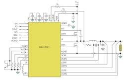
The design of dc-dc converters can get an assist from Maxim’s MAX15301 controller IC, which uses digital power technology to automatically compensate the converter (Fig. 6). It accomplishes this by constructing an internal mathematical model of the supply, including its external components.
The result is a switching power-supply design that achieves excellent dynamic performance with guaranteed stability. Furthermore, this power-supply model optimizes a converter’s efficiency across a wide range of operating conditions.
This IC relies on mixed-signal design techniques to control the power system efficiently and precisely. It doesn't require any software to configure or initialize the device. The MAX15301 can regulate and perform power-management tasks without any programming. Using standard PMBus commands, its functions can be monitored and optimized through an SMBus interface, resulting in ease of design and flexibility.
You could also use Powervation’s (now part of ROHM Semiconductor) PV3012 controller IC for a dc-dc converter design. This dual-phase digital synchronous buck controller IC for POL design applications is PMBus- and DOSA-compliant and provides features to improve a converter design’s efficiency and reliability.
The PV3012’s Auto-Control technology offers real-time adaptive loop compensation for converter designs. This patented digital control-loop technology optimizes the tradeoffs between dynamic performance and system stability on a cycle-by-cycle basis without requiring any noise injection or other drawbacks of part-time measurement techniques. This is a key advantage for converter designs that drive imprecise or variable loads.
Auto-Control also compensates for the power-supply component parameter drift that occurs over temperature and time, as well as for tolerances seen in production- or component-level variation. It relieves power-supply designers of the burden of compensation and plant characterization, while reducing total design iterations as well. Furthermore, Auto-Control readily enables efficiency maximization mode changes such as phase add/drop and light-load modes, again, without sacrificing transient performance and cost.
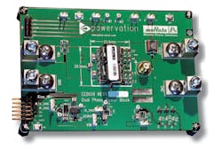
Powervation joined forces with Murata Power Solutions to co-develop a reference board for the Murata Power Solutions 45-A Power Block. Murata’s CEB019 digital dc-dc converter uses the PV3012 to overcome issues related to variations in external components, temperature, and user layouts.
