Factor PFC Into Your Power-Supply Design
This article is part of TechXchange: Power Supply Design
You can download a PDF version of this article.
Before the latest IEC61000-3-2 standard took effect in 2005, most power supplies for PCs, monitors, and TVs generated excessive line harmonics when operating from single-phase, 110- to 120-V, 60-Hz ac. Spurred on by this newer and stricter IEC standard, power-supply manufacturers aim to minimize power-line harmonics by adding power factor correction (PFC).
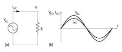
To understand the impact of IEC61000-3-2, it’s best to first look at the ideal situation, which places a load resistor (R) directly across the power line (Fig. 1). Here, the sinusoidal line current, IAC, is directly proportional to, and in phase with, the line voltage VAC. Therefore:
This means that for the most efficient and distortion-free power-line operation, all loads should behave as an effective resistance (R), whereby the power used and delivered is the product of the RMS line voltage and line current.
However, loads for many electronic systems require an ac-to-dc conversion. In this case, the load on the power line from a typical power supply consists of a diode bridge driving a capacitor (Fig. 2).
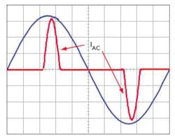
It’s a nonlinear load for the power line because two diodes of the bridge rectifier lie in the direct power path for either the positive or negative half-cycle of the input ac line voltage. This nonlinear load draws line current only during the peak of the sinusoidal line voltage, resulting in the “peaky” input line current that causes line harmonics (Fig. 3).
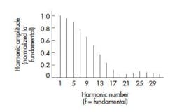
A nonlinear load causes harmonics comparable in magnitude to the fundamental harmonic current at line frequency. Figure 4 shows the magnitude of higher-order harmonics currents normalized with respect to the magnitude of the fundamental harmonic at line frequency. However, only the harmonic current at the same frequency as the line frequency and in phase with the line voltage (in this case, the fundamental harmonic at line frequency) given in Figure 1 contributes to the average power delivered to the load. These harmonic currents can affect operation of other equipment on the same utility line.
The magnitude of line harmonics depends on a power supply’s power factor, which varies from 0 to 1. A low power-factor value causes higher harmonics, while a high power-factor value produces lower harmonics. Power factor (PF) is defined as:
where P = real power in watts; IRMS = RMS line current; VRMS = RMS line voltage; and VRMS × IRMS = apparent power in volt-amperes (VA).
PF also equals the cosine of the phase angle (θ) between line current and voltage; in that regard, Equation 2 can be rewritten as:
If θ = 0°, cosθ = 1 and P = IRMS × VRMS, which is the same as for a resistor load. When the PF is 1, the load consumes all of the energy supplied by the source.
If θ = 90°, then cosθ = 0; therefore, the load receives zero power. The generator providing the power must deliver IRMS × VRMS power, even though none is used for useful work.
Thus, for the diode bridge-capacitor case in Figure 2, the only variable left in the PF definition of Equation 2 is the line current IRMS, since line voltage (VRMS) is fixed by power-line generators to 120 V. The higher the IRMS the power line draws for the given average power delivered to the load, the lower the power factor (PF). The ac-dc converter in Figure 2, which operates from 120-V ac line voltage and delivers 600 W to the load while drawing 10 A of the line current, has a PF = 0.5. However, Figure 1’s resistive load with a PF of 1, which draws 600 W from the 120-V ac line, draws only 5 A from the line.
The electric utility suffers from low PF loads because it must provide higher generating capability to support demands for increased line current due to poor load PF. Nonetheless, it charges the user only for delivery of average power in watts—not the generation of volt-amperes.
This difference between volt-amperes and watts either appears as heat or is reflected back to the AC power line. The most common means of correcting this condition is to employ power factor correction.
Power Factor Correction
The IEC-61000-3-2 standard defines the maximum harmonic current allowed for a given power level. Initial versions of the standard in 1995 and 2001 were changed by the 2005 Edition 3. It imposed stricter requirements on power-line harmonic currents for (Class D) PCs, monitors, and TVs consuming between 75 and 600 W and =16 A per phase. To meet those requirements, designers must employ active PFC in Class D power supplies.
Many PFC circuits employ a boost converter. One limitation in the conventional boost PFC converter is that it can operate only from the rectified ac line, which involves two-stage power processing (Fig. 5).
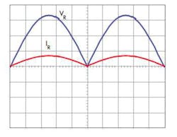
Waveforms generated by the converter better illustrate this problem (Fig. 6). In addition, there’s no simple and effective way to introduce isolation in a conventional boost converter.
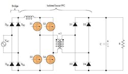
Using a full-bridge extension of the boost converter, which is then controlled as a PFC converter, is one way to introduce isolation (Fig. 7). However, this adds the complexity of four transistors on the primary side and four diode rectifiers on the secondary, both operating at the switching frequency of, say, 100 kHz. Plus, four more diodes are in the input bridge rectifier operating at the line frequency of 50/60Hz.
Besides low-frequency sinusoidal current, the line current will have superimposed input inductor ripple current at the high switching frequency, which needs to be filtered out by an additional high-frequency filter on the ac line. The presence of 12 switches operating in the hard-switching mode results in high conduction and switching losses. The best efficiency reported for this two-stage approach and its supplementary switching devices is 87%.
Such a method also suffers from the startup problem due to step-up dc conversion gain. It needs additional circuitry to pre-charge the output capacitor so that the converter can start up.
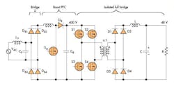
To achieve 1 kW or higher power, designers often employ a three-stage approach (Fig. 8). Here, the standard boost PFC converter and an isolated step-down converter follow the input’s bridge rectifier. This requires a total of 14 switches. At least six of those switches are high voltage, further decreasing efficiency and increasing the cost. Still, with the highest efficiency based on best present switching devices reaching about 90%, it’s better than the two-stage approach.
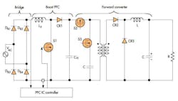
For medium and low power, there’s an alternative approach that reduces the amount of switches by using a forward converter for the isolation stage (Fig. 9). Before going this route, one must be aware that although there are now 10 switches, the four switching devices in the forward converter impose greater voltage stresses on both primary- and secondary-side switches than the full-bridge solution. In addition, the full-bridge solution requires four magnetic components.
Bridgeless PFC Converter
Breaking new ground in this arena, Dr. Slobodan Cuk, president of TESLAco, developed a bridgeless PFC converter that operates directly from the ac line. It’s claimed to be the first true single-stage bridgeless ac-dc PFC converter.
To accomplish this feat, Cuk employs a new switching power-conversion method, termed “hybrid-switching.” It employs a converter topology consisting of only three switches: one controllable switch (S) and two passive current rectifier switches (CR1 and CR2) (Fig. 10). The two rectifiers turn on and off in response to the state of the main switch (S) for either positive or negative polarity of the input ac voltage. This topology consists of an inductor in series with the input, the floating energy-transferring capacitor that acts as a resonant capacitor for the part of the switching cycle, and a resonant inductor.
Because the conventional converters based on PWM squarewave switching use inductors and capacitors, they require complementary pair switches. When one switch is on, its complementary switch is off and vice versa. As a result, only an even number of switches are allowed, compared with an odd number (three) in the new hybrid switching PFC converter.
In this setup, no such complementary switches exist. One active switch S solely controls both diodes, whose roles change automatically according to the polarity of the ac input voltage. For example, for the positive polarity of the ac input voltage, CR1 conducts during the on-time interval of switch S. Then, for negative polarity of ac input voltage, CR1 conducts during the off-time interval of switch S. CR2 also responds automatically to the state of switch S and input ac-voltage polarity. For a positive polarity, it conducts during the off-time interval of switch S; for negative polarity, it conducts during the on-time interval of switch S.
Thus, the three switches operate at all times for both positive and negative half-cycles of the input ac line voltage. Hence, this true bridgeless PFC converter operates without the full-bridge rectifier because the converter topology actually performs ac line rectification. The end result is the same dc output voltage for either polarity of input ac line voltage. Elimination of the full-bridge rectifier directly eliminates losses, especially for an 85-V low line.
The active switch S on the primary side is modulated and operated at the switching frequency, which measures three orders of magnitude higher than the line frequency (e.g., 50-kHz switching frequency compared to a low ac line frequency of 50/60 Hz). Duty ratio (D) can be defined with respect to on-time of the controlling switch S and all steady-state quantities, such as dc conversion ratios, and dc current of inductor L is expressed in terms of D.
Subsequently, the full-wave input line voltage and input line currents are sensed and sent as input to the bridgeless PFC IC controller. In turn, the controller modulates switch S on the primary side to force the input line current to be proportional to the input line voltage, providing the desired unity power factor.
This PFC converter’s truly remarkable property is that a galvanically isolated extension retains the same simplicity of the three-switch converter in Figure 10. Basically, the resonant capacitor splits into two, in series, and the isolation transformer is inserted at the point of their split.1,2
Digitally Controlled PFC
Availability of low-cost, high-performance digital controllers intended for power supplies have led to their use in PFC designs. Digital controllers provide programmable configuration, nonlinear control, low part counts, and the ability to implement complex functions that are usually difficult with an analog approach.
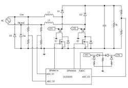
Most present-day digital power controllers, such as Texas Instruments’ UCD30203, provide integrated power-control peripherals and a power-management core, including digital loop compensators, fast analog-to-digital converters (ADCs), high-resolution digital pulse-width modulators (DPWMs) with built-in dead-time, low-power consumption microcontrollers, etc. They support a complex, high-performance power-supply design, such as a bridgeless PFC.
For example, a bridgeless PFC can incorporate two dc-dc boost circuits: L1, D1, S1 and L2, D2, S2 (Fig. 11). D3 and D4 are slow-recovery diodes. Separately sensing the line and neutral voltages referenced to internal power ground enables the input ac voltage measurement. By comparing the sensed line and neutral signals, firmware can tell if it’s a positive or negative half-cycle. During a positive half-cycle, the first dc-dc boost circuit (L1-S1-D1) is active and the boost current returns to ac neutral through D4. During a negative half-cycle, L2-S2-D2 is active and the boost current returns to the ac line through D3.
Compared with conventional single-phase PFCs using the same power devices, a bridgeless PFC and a single-phase PFC should have the same switching losses. However, a bridgeless PFC current passes only one slow diode (D4 for positive half-cycle and D3 for negative half-cycle) instead of two at any time. Thus, efficiency improvement relies on the difference in conduction loss between one diode and two diodes.
Bridgeless PFC efficiency also can be improved by turning the inactive switch fully on. For example, during a positive cycle, S2 can be fully turned on while S1 is controlled by the PWM signal. Since the voltage drop on MOSFET S2 may be lower than D4 when the flowing current is below a certain value, the return current partially or totally flows through L1-D1-RL-S2-L2 and then back to the ac source. This decreases conduction loss and improves circuit efficiency, especially at light loads. Similarly, during a negative cycle, S1 gets turned on fully while S2 is switching.
With the same input ac voltage and dc output voltage, the output current is proportional to voltage loop output. Armed with this knowledge, the frequency and output voltage thus can be adjusted accordingly. Firmware implements the voltage loop in digital controllers. Because the output is already known, it’s easy to implement this feature, and less costly than an analog approach.
More Digital Control
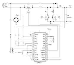
Analog Devices' DP1047 and ADP10484 digital PFC controllers also provide input power metering and inrush current control. The ADP1047 is intended for single-phase PFC applications, while the ADP1048 targets interleaved and bridgeless PFC applications.
The digital PFC function is based on a conventional boost circuit to provide optimum harmonic correction and power factor for ac-dc systems. All signals are converted into the digital domain to maximize flexibility; key parameters can be reported and adjusted via a PMBus interface.
Overall, the ADP1047 and ADP1048 were configured to help designers optimize system performance and maximize efficiency across the load range. The two ICs accurately measure RMS input voltage, current, and power. Then that data can be reported to the power supply’s microcontroller via the PMBus.
The ADP1048’s bridgeless boost configuration allows for removal of conduction losses caused by the PFC converter’s input bridge (Fig. 12). In this configuration, the two power MOSFETs must be driven separately to achieve the highest efficiency. Signals from the ADP1048 make this possible. The IBAL pin detects the ac line phase and zero crossings. The maximum rating on the IBAL pin is VDD + 0.3 V, so it needs to be protected with a suitable clamp circuit.
During the positive ac line phase, only one boost stage is effectively working. The second stage is passive; the current flows in Q2 from the source to the drain. Turning the Q2 FET fully on during this phase minimizes conduction losses in Q2. When the ac line phase becomes negative, the roles of Q1 and Q2 are reversed, and Q2 switches actively while Q1 is always on. The phase information is detected from the ac line via the IBAL pin. During the soft-start phase, both FETs switch as a precautionary measure. The same situation happens when phase information on the IBAL pin becomes corrupted or inaccurate.
Read more articles in TechXchange: Power Supply Design
References
- Cuk, Slobodan, “True Bridgeless PFC Converter Achieves Over 98% Efficiency, 0.999 Power Factor,” Power Electronics Technology, July 2010.
- Cuk, Slobodan, “True Bridgeless PFC Converter Achieves Over 98% Efficiency, 0.999 Power Factor, Part 2,” Power Electronics Technology, August 2010.
- Bosheng Sun and Zhong Ye, “Digital Control Improves Bridgeless PFC Performance,” Power Electronics Technology, March 2011.
- Analog Devices ADP1047/ADP1048, “Digital Power Factor Controller with Accurate AC Power Metering” data sheet, September 2011.
