EMI Reduction Techniques for Op Amps
This article is part of the TechXchange: Delving into EMI, EMC and Noise
Members can download this article in PDF format.
What you'll learn:
- Op-amp performance is disrupted by EMI in a variety of ways.
- Reducing EMI in amplifiers using filters.
- How to mitigate EMI in Class-D audio amps.
In this article, electromagnetic interference (EMI) will be discussed as it relates to operational amplifiers (op amps) and other amplifiers. We will examine EMI effects on op amps/amplifiers, an EMI filter that uses an op amp, op amp EMI rejection ratio (EMIRR), an EMI-hardened op amp, minimizing RF EMI interference in amplifiers, EMI in Class D audio op amps, EMI damage to bipolar transistors in op amps, and more.
EMI Effects in Op Amps/Amplifiers
EMI can disrupt op-amp performance in multiple ways. Engineers need to first identify the type of injection (conducted, radiated, common mode, differential mode) and the coupling point location. One means of entry into the device involves EMI coupling into the pins of the op-amp integrated circuit (IC).
When this happens, the cause of disruption to the op amp will be due to rectification, which will change the bias point of the device. The most profound effect in the op amp, from this EMI intrusion, will be interference with the dc component that can wreak havoc inside the device.
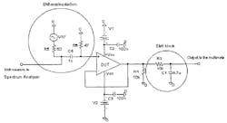
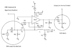
We will look at one method of injection to the device: a conducted injection between each pin of the IC and the ground (this will cause differential-mode noise). Experimental results show that in several cases, EMI can cause degradation of op-amp behavior.1 Figures 1 and 2 illustrate the measurement setups used for “constant frequency” and “constant voltage” measurements, respectively.
A numerical approach to predict EMI effects on ICs, using simulation, is evaluated with successful and consistent results that were very close to measurement results. Reference 1 has more details.
An EMI Filter Using an Op Amp
Integrated power electronic modules (IPEMs) need small size and high performance with good power density. Typically, IPEM architectures use passive filters with relatively narrow bandwidth. Employing magnetic cores in this kind of design architecture presents a challenge in size, weight, and temperature, as well as reliability. This method often doesn’t perform the necessary job of good noise elimination in modern electronics systems.
The AEF
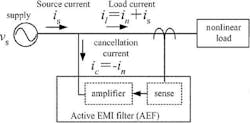
An interesting design architecture for EMI is the active EMI filter (AEF)2 for an IPEM. It can replace a large passive EMI filter with small passive components coupled with an active op-amp circuit (Fig. 3).
This kind of design technique is suggested when improved attenuation is needed at relatively low frequencies while easily meeting high-frequency filtering requirements. The number of passive components in this architecture are minimized. The filter EMI noise spectrum is typically from 150 kHz to 30 MHz according to the CISPR22 EMC standard.
The power rating of the AEF is very small, so it doesn’t need to use a switching mode technique. The linear mode performs the task well enough.
Op-Amp EMIRR3
Texas Instruments, for example, is addressing EMI immunity by designing op amps and other linear devices with input EMI filters to increase EMI immunity. These op amps, which are EMI-hardened, will provide extra EMI protection to circuitry such as in AEFs.
Minimizing RF EMI Interference in Amplifiers
One of the main offenders of EMI interference among electronic devices are mobile devices. Radiated EMI will enter susceptible traces and devices on a printed circuit board (PCB) and wreak havoc on devices such as op amps and other amplifier circuitry. EMI will intrude into a system through conduction over power and signal traces on the PCB. The length of traces on a PCB become good antennas at RF and microwave frequencies.
Switching power supplies may be one of the most offending architectures in a design. Other common sources of conducted interference are ac motors, digital circuitry, and microcontrollers.
The use of EMI filters can help ensure proper operation in a harsh EMI environment. These filters will help suppress conducted signals on power and signal traces. EMI filters may be external on a PCB or may even have integrated EMI filters within an IC. The use of differential- or common-mode filter designs may be used on a PCB to filter out common-mode EMI coupling and/or differential-mode EMI coupling.
Common-mode EMI coupling takes place when the offending EMI noise has the same phase in two adjacent conductors. Differential-mode coupling EMI coupling occurs when the noise is out of phase on two adjacent conductors.
There are two forms of induced coupling (inductive coupling occurs when the EMI “offending source” has a common ground with the “victim”)—capacitive and magnetic:
- Capacitive coupling occurs when the voltage in a conductor changes and creates a voltage that can couple with a nearby conductor, inducing an offending voltage into it.
- Magnetic induction occurs when the parasitic magnetic field gets transferred between a source and a victim. The changing current in a parasitic magnetic field transfers from the source to the victim.
EMI Reduction in Class-D Audio Amplifiers
Consumer and portable electronic designs are ever-shrinking in size. Thus, designers are forced to eschew metal shields to minimize EMI. In addition, PCBs are approaching higher and higher densities with the use of wafer-scale packages. As a result, EMI is much more difficult to tame in these modern architectures.
Many electronic architectures use antennas to receive and transmit signals. However, “unintended” antennas on a PCB are long copper trace runs, vias, component leads and pins, and connector and header devices on an unpopulated PCB. Surface and buried traces that aren’t terminated may act as whip antennas. Even the conductive layers of a multilayer PCB may act as the other leg of a dipole antenna with the plane itself getting coupled into the electric field.
Let’s take a look at the high-efficiency Class-D amplifier that modulates a high-frequency square wave via the incoming analog signal to the amplifier. Two-pole Butterworth filters are typically employed to filter out the unwanted high-frequency content while recovering the wanted audio signal.
Pulse-width modulation (PWM) is a common Class-D topology. It uses a fixed frequency waveform and changes the duty cycle to create a moving average of that signal after a low-pass filter (Fig. 4).
Effective Reduction of EMI in a Class-D Op Amp
The best way to plan an effective EMI reduction for the Class-D amp is at the PCB level:
- In general, strategic placement of decoupling capacitors between ground and points where voltage fluctuations are likely to occur.
- Power ground planes should avoid being near the edges of the PCB.
- Try not to use traces that are cut into ground or power planes; these are unintended apertures susceptible to EMI.
- Terminate all high-frequency clock lines.
- Apply good filtering at PCB connectors.
- Avoid loop antennas with copper traces.
- If driving a loudspeaker, add a series ferrite bead at the amplifier output.
EMI Damage in BJTs
Damage of bipolar transistors (BJTs) via high power microwave (HPM) radiation6 could affect their response to EMI and change an op amp’s electromagnetic susceptibility5 (EMS). The work in Reference 5 investigated the effect of hot-carrier stress on a BJT’s response to EMI. The experimental results demonstrated that the transistor base current increased under EMI and the amplitude increases after hot-carrier stress. When the base terminal is biased by a current source, the voltage across the emitter-base junction drops more significantly after hot-carrier stress.
During hot-carrier stress, the damage will be localized close to the emitter-base junction that, in turn, will cause the excess base current to have an ideality factor of two (ideality factor is a means of measuring how accurately the diode follows the ideal diode equation). The ideality factor n will vary from one to two (it may be higher in some cases, though), depending on the fabrication process and semiconductor material, and it’s set equal to one for the case of an "ideal" diode (thus the n is sometimes omitted). The ideality factor was added to account for imperfect junctions as observed in real transistors.
Summary
This article has brought to light some harmful effects that EMI can have on op amps/amplifiers. Readers will learn how to minimize/prevent EMI and possible damage to op amps in their designs. EMI filter designs also are included. This will help designers create more robust designs, leading to better lifetime and performance in their designs.
Read more articles like this at the TechXchange: Delving into EMI, EMC and Noise
References
1. “Analysis of EMI Effects in Op-Amp IC’s: Measurement Techniques and Numerical Prediction,” IEEE 2001
2. “An Active EMI Filtering Technique for Improving Passive Filter Low-Frequency Performance,” IEEE Transactions on Electromagnetic Compatibility, Vol. 48, No. 1, February 2006
3. “EMI Rejection Ratio of Operational Amplifiers,” Application report 2015
4. Design with Operational Amplifiers and Analog Integrated Circuits, Fourth Edition, Sergio Franco
5. Hot-carrier effect on the bipolar transistors’ response to electromagnetic interference, Microelectronics Reliability, Volume 55, Issues 3–4, February–March 2015, Pages 514-519
6. “Electromagnetic Inteference by High Power Microwaves,” Proceedings of International Conference on Electromagnetic Interference and Compatibility (INCEMIC) 2001 - 2002


