Circuit Meets Challenges Of Fast, High-Current NiCd Charging
This article is part of the Ideas for Design Series: Vol. 3, No. 1
Batteries based on the nickel-metal-hydride (NiMH) and lithium-ion (Li-ion) chemistries have largely replaced the older nickel-cadmium (NiCd) battery in many of today’s applications. Still, NiCds are the preferred choice when high discharge currents and a rapid recharge cycle (between one and two hours) are principal concerns.
Related Articles
- Intelligent NiCd Charger Avoids Battery Damage From High Currents
- SImple NiCd Battery Charger Includes Charge Indication
- A Complete Battery Backup Solution Using A Rechargeable NiCd Cell
Precautions must be taken, however, when you try to recharge a standard NiCd cell “fast” at current levels that approach or exceed the rated capacity of the battery (called its C-rating). As the battery becomes fully charged, these high-current levels (at 1C or higher) cause a rapid increase in electrochemical reaction (oxidation/reduction) within the cell, with a corresponding rapid increase in both internal cell pressure and temperature.
Therefore, as the cell approaches or exceeds 100% capacity, the high charging current must be reduced or the cell’s overcharge safety vent may open, causing gasses to escape with a possible loss of electrolyte. Additionally, repeated overcharging could degrade the cell’s life—the useful number of charge/discharge cycles—or even render it permanently useless.
One way to avert the potential damage that can result from repeated cell overcharging at high currents is to monitor the differential temperature TDIFF = TB – TA between the battery’s surface temperature (TB) and ambient temperature (TA) and proportionally reduce or “taper” the charging current ICH as the differential temperature increases.
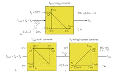
Consider a design that must convert a differential temperature rise (battery surface temperature above ambient) that ranges from 0°C to 5°C into a charging current that decreases proportionally from a maximum current level of 1C to 0 A. If the rated capacity of an AA cell equals 600 mAhr, then 1C equals 600 mA. Equation 1 describes this differential-temperature-to-charging-current system:
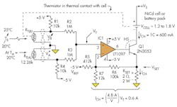
Temperatures TB and TA are monitored separately by standard negative-temperature-coefficient (NTC) thermistors (10 kΩ at 25°C) with corresponding resistance values of RT(B) and RT(A), respectively (Fig. 2). Both sensor output voltages, VB and VA, are then applied to the inputs of a basic passive adder created by R2 and R3. At TB = TA = 20°C (i.e., TDIFF = 0°C) VB = +2.75 V and VA = -2.75 V, the passive adder’s output voltage is given by single-ended control voltage VT = (VA + VB)/2 = (–2.75 V + 2.75 V)/2 = 0 V.
When TB rises to 25°C due to the initial high charging current of 600 mA and TA remains constant at 20°C (TDIFF = 5°C), the sensor voltage VB = +2.50 V and VA = –2.75 V while control voltage VT = (VA + VB)/2 = (–2.75 V + 2.50 V)/2 = -0.125 V. As a result, the output of the passive adder produces a value for VT that is inversely proportional to TDIFF, (Fig. 1b):
The voltage-to-high-current converter circuitry around IC1, whose output current is directly proportional to VT, has both scale and offset capabilities and therefore can be designed to deliver the needed charging current ICH to the battery (Fig. 1c). Circuit performance is described analytically by:
Before proceeding, we can check the validity of this design by convolving Equation 2 with Equation 3 to reproduce Equation 1:
Begin the design implementation with TDIFF at 0°C where VT = 0 V. VSET is chosen to equal 1.25 V, the maximum charging current is set at 600 mA, and the RSET resistor value is determined by letting RSET = VSET/ICH = 1.25 V/600 mA = 2 Ω (2 W). When the differential temperature TDIFF rises to 5°C and VT = -125 mV, the value of VSET will have linearly decreased to 0 V, causing ICH to drop to approximately 0 A, terminating the high-current charge. The performance equation for this voltage-to-high-current converter is given by.
However, dividing both sides of the equation by RSET yields the more useful form for design:
Final component selection for this converter is accomplished by comparing both offset and scale terms of the design equation (Equation 3) with the converter’s corresponding performance equation terms in Equation 4b. Set feedback resistor R6 to 100 kΩ, 1% and equate offset terms in Equation 5. Then solve for the value of R5 by choosing –5 V for VREF.
The calculated value of R5 (416.67 kΩ) is approximated by choosing a standard 412 kΩ, 1% resistor. Finally, calculate the value of R7 by comparing scaling terms in.
The calculated value of R7 is 11.96 kΩ, which can be satisfied with a standard 12-kΩ, 5% resistor. Circuit performance was simulated and verified by laboratory measurement over multiple charge/discharge cycles.
Reference
Villanucci, Robert S. and Diecidue, Joseph, “‘Intelligent’ NiCd Charger Avoids Battery Damage from High Currents,” Electronic Design, May 8, 2008, p 51-54, http://electronicdesign.com/power/intelligent-nicd-charger-avoids-battery-damage-high-currents
Read more articles from the Ideas for Design Series: Vol. 3, No. 1
Robert S. Villanucci, professor (retired), holds an AEng from the Wentworth Institute of Technology, Boston, Massachusetts, a BSET from Northeastern University, and an MSEE from Tufts University, Medford, Mass.
Joseph Diecidue, electronics technician, holds a BSEE from the Wentworth Institute of Technology, Boston, Massachusetts.
About the Author
Robert Villanucci
Professor (retired)
Robert S. Villanucci, professor (retired), holds an AEng from the Wentworth Institute of Technology, Boston, Mass., a BSET from Northeastern Unviersity, and an MSEE from Tufts University, Medford, Mass.
Joseph Diecidue
Electronics Technician
Joseph Diecidue, electronics technician, holds a BSEE from the Wentworth Institute of Technology, Boston, Mass.
Voice Your Opinion!
To join the conversation, and become an exclusive member of Electronic Design, create an account today!

Leaders relevant to this article:


