Download the "What's All This Algebraic Equation Stuff, Anyhow?" eBook.
Article updated 10/04/22
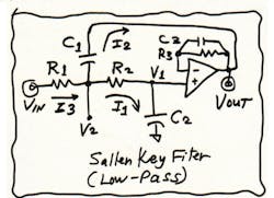
As we were saying, it can be tricky to figure out a filter, yet not impossible. Let's take the example of a basic Sallen-Key filter—the low-pass one in the figure. Do we have to worry about R3 and C3? No, they're only needed to prevent bad offset due to the bias current of a bipolar op amp. For any decent FET op amp, R3 should be 0 and there is, of course, no need for C3. They have no effect on the response anyway.
Let's say we acknowledge that when the input signal moves, there will be currents (such as I1, I2, and I3) flowing, and voltages (such as V1 and V2) moving. How can we analyze this to see the overall response of the filter? If you just start writing equations, it's easy to crawl into a morass that does not lead to an answer—which I have done many times. But here's an approach that I've used many times successfully.
In this case, let's assume that we know VOUT, and work back to the front of the circuit. If we know VOUT, then it's reasonable to assume that V1 @ VOUT, given a finite bandwidth for the op amp, so the bandwidth is much more than F3dB. (If that's not the case, I will let you factor it in, that V1 = VOUT × (1+p/ωh).) Then the current I1 will be VOUT × pC2, where 1/pC2 is the impedance of the capacitor and p is the derivative operator d/dt. (Later, we may substitute in that p = s = 2πjf (or jω).)If we know that I1 = VOUT × pC2, then we know that V2 is I1 × R2 higher than VOUT, so V2 = VOUT + I1 × R, or V2 = VOUT + VOUT(pC2R2). That's good information because now that we know V2, we can compute that:
I2 = (V2 − Vout) × pC1 = VOUT × p2C2R2C1
Now that we know I2, we know that I2 + I1 = I3 , and the input voltage V1 will be (I1 + I2) × R1 bigger than V2. Let's stuff this all into a big equation:
VIN = VOUT × [1 + pC1(R1+R2) + p2R1C1R2C2]
The result is that VIN = F × VOUT. This shows that the VIN is normally bigger than VOUT by that factor. So the useful result is:
VOUT / VIN = Gain = 1 / [1 + pC1(R1+R2) + p2R1C1R2C2]
Now we have shown that it's possible (I never said it was easy) to compute the frequency response of a simple RC filter with two Rs and two Cs.
This indicates that it would be possible to compute the response of analog filters with three or more Rs and three or more Cs. Not a big deal. You may use several sheets of paper, but you can get there, if you are meticulous. (In the previously noted filter with the twin Tee, there were about 16 terms, each with an average of six items, so the number of places where you can goof up is not small, but you can do it.)
If you maintain the product of R1C1R2C2 constant, the f20dB and high-frequency rolloff will stay about the same. But increasing C1 while decreasing C2 can cause peaking in the frequency domain, overshoot for step response in the time domain, and even ringing. This is especially true for C1(R1+R2) > 1.4√R1C1R2C2. Fool around and see for yourself! More on this later in Part 4.
Should you have the same quality of C for C1 and C2? Nope. C1 should be a pretty good capacitor; mylar or metalized mylar may be suitable. But C2 has to be a low-leakage type, such as polypropylene. (C1 does not.) So C2 should be of good quality, and C1 can be cheaper. There's never any dc voltage on C1. Its leakage characteristics are not important. Neither is its soakage.
Beware of using any LM324 output stages. That can cause poor linearity and poor rejection. A preload could help. Most LM324 computer models don't tell the truth about this.
This isn't the only filter in the world, but there are many filters just like it and they have the same shape. This filter has no need for precision resistors, as they don't affect the gain. However, CM slew and CMRR nonlinearities and CM input impedance (capacitance) aren't always trivial matters. But many people like this, as I do for many cases.
All for now.
This article was published in Electronic Design Nov 5, 2001
see Bob Pease Remembered — One Year Later
This is how Bob always ended his blog. The information is no longer valid.
/ Comments invited!
RAP / Robert A. Pease / Engineer
[email protected]—or:
Mail Stop D2597A
National Semiconductor
P.O. Box 58090
Santa Clara, CA 95052-8090


