The semiconductor industry is moving out of the monolithic age of the system-on-chip (SoC).
Instead of arranging every building block of IP on the same slab of silicon, the movers and shakers in the chip market are breaking them down and bundling them into separate smaller chiplets. Each of these smaller chiplets can be made using the most optimal process technology for the job in the system. Integrating all of the chips together with 2.5D packaging or 3D integration makes it possible to mimic a single large chip.
In principle, companies could take care of the chiplets at the heart of the processor—for instance, chiplets for general-purpose computing based on CPU cores, or those housing high-performance accelerators such as GPUs. Then they could choose off-the-shelf chiplets for the memory, connectivity, or other features. But, in practice, most companies construct the chiplets by themselves due to the cost and complexity of adopting third-party chiplets and the limited standards surrounding them.
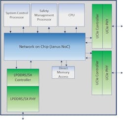
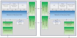
Cadence is trying to reduce the design complexity for chiplet technology with what it called the first system chiplet. The company said it taped out the new system chiplet, which is specifically designed to serve as the central controller in the package, managing all of the resources and functionality of the multi-chiplet SoC. Developed with Arm, it communicates with the other chiplets in the package over the Universal Chiplet Interconnect Express (UCle) interface.
Cadence is one of the leading players in electronic design automation (EDA) tools used to design, simulate, and prototype chips. But it also develops many of the smaller building blocks of IP and other blueprints that are slotted into modern processors. Cadence said the system chiplet integrates Arm’s processor IP with its system, memory, and interconnect IP and PHYs in a single die. It’s also one of the first chiplets to comply with Arm's Chiplet System Architecture (CSA).
There are different ways to disassemble a large heterogeneous SoC into several smaller chiplets and reassemble them in a system-in-package (SiP). On that front, Arm is collaborating with Cadence and others to create a more standard approach to partitioning chiplet-based designs, enabling broader reuse of physical design and other types of IP. Arm said CSA is all about dividing complex systems into modular chiplets in the same way a monolithic chip is composed of IP blocks.
By bundling system, safety, and memory controllers and other building blocks of IP into a separate system chiplet, Cadence said it hopes to help chip designers bring new processors to market faster.
Chiplets: The Wave of the Future for Heterogeneous SoCs
The semiconductor industry is shifting to chiplets to solve some of the challenges faced by heterogenous SoCs, which are becoming prohibitively costly and complex as Moore’s Law slows down.
The shift to a chiplet-based approach to semiconductor design brings several benefits to the table:
- Scalability: By spreading out all processor subsystems over several chiplets, companies can cram more transistors in a single package than is possible in a single die, significantly driving up the performance. The latest AI chips contain as much as 2,500 mm2 worth of silicon when assembled with 2.5D packaging technologies, which is about 3X larger than the reticle limit of the largest chips being fabricated, which are up to approximately 850 mm2 today.
- Flexibility: Each chiplet in the package can be produced on the best process technology for its job, giving engineers more flexibility to optimize the power, performance, and area of each chiplet in the SiP. The most advanced nodes are becoming more expensive per transistor, which raises the question of whether it makes sense to upgrade every chip in the package to the latest node.
- Modularity: The mixing and matching of different chiplets also opens the door to custom silicon for companies that traditionally have been locked into commercial off-the-shelf products. It also gives them the ability to adapt more rapidly to technological advances in areas such as machine learning. One of the other prospects for chiplets is composability, or the ability for companies to reuse chiplets from other products or various other vendors and even bring industry standard into the package.
That’s also the goal of the UCIe standard, which is one of the front-runners in the race for a high-bandwidth, die-to-die interconnect that enables third-party chiplets to communicate with each other in the system.
Arm is trying to build its high-performance CPU cores and other IP into the central compute tiles at the heart of the package, and it’s supplying more of a complete and pre-validated set of blueprints for its CPU cores called Compute Subsystems (CSS) to lessen the complexity for customers. The company is also collaborating with Cadence and others in the semiconductor market to roll out chiplet-based reference designs for the various chiplets piled into the package.
>>Check out this TechXchange for similar articles and videos
The Chiplet System Architecture (CSA) is all about working with the broader industry to agree on a standard set of chiplets—for computing, memory, connectivity, or any other functions—and the role that each one plays. The goal is to give companies a template for the chiplets in the package and then, depending on their requirements, they can slot in-house or third-party IP into the appropriate chiplet.
However, the reality is that a wide range of technical challenges exist with chiplets, requiring advances in everything from advanced packaging to power distribution and heat dissipation.
Inside Cadence’s System Chiplet: System, Memory, and Safety Controllers
Cadence said the system chiplet contains system control and safety management processors based on Arm CPU cores, along with its PHY and controller IP for connecting to memory over LPDDR5 and to other chiplets in the package over UCle.
In most cases, modern chips have a separate processing unit that’s specifically designed to manage all of the different components in the heterogeneous SoC. It serves as a central control unit for the larger processor.
The system manager takes care of power management by dynamically adjusting power based on the system’s load or alternating between different power states; it controls the clock speeds of the different components to adjust performance and power use. The system manager also tracks the chip’s temperature and takes steps to prevent overheating, such as throttling the processor’s speed. It’s used to control the secure boot and loading of the operating system along with other system monitoring tasks.
In other cases, modern chips contain another processing unit used to run diagnostics on the system to prevent faults caused by the hardware or software before they lead to catastrophic failures. These safety managers are also present in autonomous-driving chips to isolate safety-critical code from application software that runs in the same heterogeneous SoC. They’re integral to the latest safety standards such as ASIL D.
Based on its Janus NoC technology, Cadence said the Arm-based system chiplet can accommodate up to 64 GB/s of connectivity bandwidth over UCIe and 32 GB/s of peak memory bandwidth for the LPDDR5 controller IP.
Ultimately, it’s unclear whether companies will want to use Cadence’s system chiplet as is, leveraging all the same system, safety, and memory controller IP. But if nothing else, it gives them a blueprint for building a system chiplet of their own.


