Increased device complexity can be addressed by providing parallel test while decreasing the throughput overhead of the ATE architecture.
The consumer world is converging, and the lines between consumer, computation, and communications applications continue to blur as more and more functionality appears in each consumer device. For example, cell phones, only one type of device, now include digital cameras, video, Internet and e-mail access, multimedia gaming, short message services, multimedia messaging, MP3 players, digital radio, location services, PDA capabilities, and even broadcast TV.
The higher-quality audio and video applications coming to the cell phone require faster sampling rates, wider dynamic range, and an increase in memory. Even in the confines of automobiles, demand for higher-quality audio and video is increasing with multichannel audio and high-resolution location displays using global positioning system (GPS) receivers with DVD information storage.
The major consequences of this consumer-application convergence are increased system-level integration of RF, mixed signals, high-speed interfaces, power management, memory, and powerful processing. To keep size, cost, and power consumption low, these devices are being manufactured as a system on a chip (SOC) or as a system in a package (SIP). As the functionality and number of different cores increase, so does the number of digital pins to accommodate the needed digital control and data lines.
Industry-Specific Test Demands
The increase in SOC and SIP complexity in the high-volume consumer world conflicts with two fundamental requirements: low cost and shorter device life cycles. Consumers want more performance at the same or lower cost, and they�re demanding new improvements more often. The parts must be tested thoroughly but very quickly at low cost.
The additional time to test increased device complexity can be addressed by providing greater parallelism in test while significantly decreasing the throughput overhead of the ATE architecture. To address the challenges of the analog cores now appearing in the leading-edge consumer devices, both of these enhancements must be enabled while maintaining the resolution and accuracy of the ATE hardware.
Audio DAC and ADC
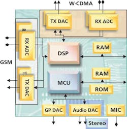
Highly integrated SOC devices, such as the cellular baseband processor in Figure 1, include multiple disparate functional blocks that can be challenging from both a specification and a test time perspective.
Figure 1. Baseband Processor Block Diagram
The audio quality requirements of previous generations of cellular phones typically could be met by simple digital-to-analog converters (DACs) and analog-to-digital converters (ADCs) with 10-b effective resolution and 4-kHz bandwidth. The current trends toward CD-quality audio performance, stereo, and surround-sound capability are supported by devices with much more stringent specifications. Although referred to as 24-b audio, the actual effective performance generally is 16 b to 17 b, corresponding to a 98-dB to 104-dB dynamic range with a bandwidth of 20 kHz.
Discrete CD-quality DACs and ADCs are used in consumer devices, but the cost of ATE associated with testing these devices is manageable because the devices command relatively high prices. Integrating CD-quality cores in an SOC increases test time because of the additional functionality and adversely affects the cost of test (COT), which can�t be offset by an increase in device price.
Example Derivation of Test Time of Audio Core
For mixed-signal dynamic testing, it is critical to obtain a coherent measurement to prevent spectral leakage in the resulting spectrum used for analysis. As a result, the following relationship must be met:
Where M = number of cycles captured
N = number of points sampled
Ft = frequency of test signal
Fs = frequency of sampling
For lower fidelity audio devices, such as the microphone input ADC or the earpiece output DAC, an 8-kHz sampling frequency is used corresponding to the 4-kHz bandwidth. With a 1.03125-kHz test signal, an ADC with a sampling frequency of 8 kHz and a 512-point acquisition, 66 cycles are captured. The sampling time equals the number of points divided by the sampling frequency:
Audio testing requires 10 or more tests including multiple gain states, idle channel noise (ICN), crosstalk (XTALK), and intermodulation distortion (IMD), resulting in an overall time of approximately 650 ms for these very simple cores.
Transferring 20-b sample data from the ATE�s analog or digital capture memory to the workstation can create a significant test-overhead impact. To determine the amount of data that will be transferred for analysis, multiply 20 b by the number of points sampled (N) by the number of measurements made to test the core.
In our example, 20 b � 512 points � 10 measurements or 102,400 b are transferred. Assuming a 1-Mb bandwidth between the analog module and the workstation, the transfer time to test the DAC core would be approximately 100 ms. Given the same bandwidth for the digital capture memory transfer, the overhead also would be 100 ms. The 200-ms transfer overhead increases the total test time to 1,500 ms (650 ms + 650 ms + 200 ms) for a voice-quality DAC and ADC test.
ATE Architecture Overhead in Parallel Test
Considering the impact of a surround-sound audio processor on test time will further illustrate the problem. From the analog perspective, these devices require a combination of high dynamic range and parallelism. AC3 digital audio provides six analog outputs: front L/R, surround L/R, center, and subwoofer.
CD-quality dynamic range and bandwidth require a higher sampling rate. Using the above formula but with Fs = 48,000 Hz
Adding in the times necessary for settling, hardware setup, and other overhead, the test time is approximately 15 ms. The total test list again would include 10 or more, resulting in a test time of 150 ms. Given six channels, a serial test implementation would require 1,500 ms per site.
A quad-site implementation could take advantage of multiple waveform digitizers to affect parallelism. But, data transfer overhead still is generally serialized in multisite test, so the overhead would be cumulative. A quad-site test implementation, even with four waveform digitizers, would require 900 ms + 4 � 600 ms = 3,300 ms.
Multiple-Standard Cellular Baseband Processors
Cellular devices are incorporating multiple standards within the same phone. To support these multiple standards, the chipset often has redundant baseband analog converters as well as RF transceivers.
As in the audio-surround processor, the numerous analog cores in the cellular baseband processor create a significant impact on test time. The major challenge in testing these devices is to incorporate sufficient parallelism in the analog test hardware to achieve multisite efficiency.
The baseband processor block consists of in-phase/quadrature (I/Q) transmit (TX) DAC and receive (RX) ADC pairs. In 2G to 2.75G GSM/GPRS/EDGE technologies, the carrier channel spacing is limited to 200 kHz, leading to a low-frequency Zero-IF requirement. W-CDMA uses a 5-MHz channel spacing corresponding to a much higher bandwidth.
Full dynamic testing of the RX and TX paths generally is required, including signal to distortion (SND), ICN, and XTALK. The I/Q-paired DACs and ADCs also require gain-match and phase-match testing, usually to specifications as tight as 0.1 dB and 3 degrees, respectively.
The need to maintain channel isolation during transmission leads to additional out-of-band (OOB) attenuation testing for the DACs. The adjacent channel power ratio (ACPR) test confirms channel isolation and requires that OOB frequencies up to 10 MHz are verified for the W-CDMA DACs.
High-Definition Video Encoder
Multiple video input standards are supported by current SOC devices. Traditional NTSC or PAL devices incorporate super video (S-Video) and composite analog outputs. Support for HDTV requires three additional outputs to provide the YPrPb HDTV (EIA-770.1-3) compliant signals. To incorporate all of these outputs requires six video DACs: two for S-Video, one for composite, and three for RGB.
Although the interface speed for the most challenging of the digital video standards is approximately 74 MHz, the analog bandwidth required to test the DAC performance is approximately 8 MHz with 10-b to 12-b resolution. A typical test plan for individual video DACs includes integral non-linearity (INL), differential non-linearity (DNL), and SND measurements. But the picture quality of the HDTV system also is determined by the relative accuracy of the DAC outputs, which necessitates additional testing of the output gain and phase matching.
The overall test time of a device incorporating digital video directly correlates to the number of parallel digitizer units available for test. As there usually are six or more video DACs to test, it often is necessary to create a serialized test approach due to the lack of tester resources.
Addressing Parallel Testing
Although reduction of the overall COT is influenced by many variables, improving throughput by implementing multisite and concurrent test is a primary method. The newest generations of ATE systems use a multiport architecture that supports configuration of groups of tester resources to match the function of the device under test.
The two primary functions required to enable this are a per-port timing generator to match the frequency of test to the core and a per-port sequencer that allows the port to operate in different test modes and execute autonomous sequencer instructions. Per-pin multiport takes this a step further by providing the granularity of the configuration to each pin of the ATE system for both digital and analog resources.
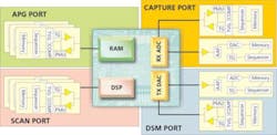
An example of the configuration of resources necessary to test a typical communications SOC includes a digital signal processor (DSP) acting as a communications processor, memory, and ADCs and DACs to interface to the analog IF or RF front end. In this case, one port of digital pins can be configured in the algorithmic pattern generation (APG) mode for the memory test and another group of digital pins in the scan mode to test the DSP core (Figure 2).
The ADC block will require an arbitrary waveform generator (Arb) as well as digital channels in the capture mode to acquire and analyze the results of the analog to digital conversion. The DAC needs a port consisting of digital channels for the digital source memory (DSM), or waveform memory segment, and a waveform digitizer. Each of these ports must operate autonomously at different test frequencies and with different sequencer instructions.
Because the test system already is segmented on a per-pin basis, the application software automatically can manage most of the multisite control by duplicating images of the test vectors and sequences across pins that are used per site.
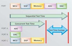
Concurrent test is an extension of multiport test that allows these cores to be tested in parallel. Each core in the device must be independently accessible and controllable by the ATE system and act independently. Test execution time is reduced by modifying the flow from purely sequential, where each device core is tested serially, to a flow where multiple device cores are tested in parallel (Figure 3).
Figure 3. Concurrent vs. Sequential Test Time Savings
In large-scale devices, such as the Cellular Baseband SOC processor, there are numerous analog cores, and testing these cores in parallel requires a large number of analog resources. To test the device in a quad-site, fully parallel, concurrent test mode, it is necessary to provide 28 digitizers. This is not realistic in today�s ATE systems.
A New Analog Module Architecture
A highly parallel, low-overhead solution is needed to test the diverse analog cores found in today�s consumer devices. By combining several analog functions into one module, less space is taken by individual analog modules, opening up more room for needed digital modules.
A module incorporating eight individual Arbs or digitizer units offers the benefit of flexible configuration: either digitizer-only units or a combination of digitizer and Arb units is possible.
Reducing COT in consumer device testing requires not only addressing the parallelism of the ATE test system, but also the ATE overhead associated with this parallelism. Architectural improvements of ATE hardware must take both points into consideration to best address test of the numerous cores that comprise today�s SOC consumer devices.
About the Authors
Jeff Brenner is a principal mixed-signal test consultant with the Agilent Technologies Automated Test Group. He holds a B.S.E.E. in electrical engineering and has 10 years of experience in the semiconductor test industry. Agilent Technologies, 12401 Research Blvd., Bldg. I, Suite 100, Austin, TX 78759, e-mail: [email protected]
Gordon J. DeWitte is a product manager in the Consumer and Wireless Solutions Test Division of the Agilent Technologies Automated Test Group. He joined Agilent/HP in 1984 and, from 1993 to 1999, was the product manager for external sales of microwave and millimeter-wave GaAs ICs manufactured at the Microwave Technology Center. Mr. DeWitte received a B.S.E.E. degree from Massachusetts Institute of Technology. Agilent Technologies, 1400 Fountaingrove Parkway, M/S 3LSW, Santa Rosa, CA 95403, 707-577-3887, e-mail: [email protected]
Audio Video 8
(AV8)
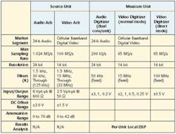
The Agilent Technologies AV8 Module shares the water-cooled, constant-temperature environment of the 93000 SOC Tester, which ensures consistent, drift-free performance. The 93000 test head supports up to 64 modules. Each digital module is composed of 16 per-pin channels. A standard configuration supports up to 25 analog modules. The AV8 analog module provides eight units.
Each source unit consists of two Arb cores, an Audio Arb and a Video Arb, and an integrated Precision DC Measurement Unit (PMU). These two cores share a common output and are selectable on a per-test basis during the execution of the device test flow.
The measure unit consists of a dual-channel audio digitizer, a video digitizer, and an integrated PMU. Within each measure unit is a DSP for local results processing. Table 1 shows typical module deployments required for three types of devices.
