Although it requires a new generation of test equipment, testing MEMS devices is challenging but not impossible.
Since the early days of the IC industry, wafer-level test has been possible using precision-controlled wafer probers to step from die to die on the wafer, making electrical contact using needle probes. Over time, the requirements to accomplish this testing have become more severe, requiring more sophisticated probers and probe cards. While challenging, these requirements have been met using available technology.
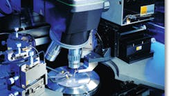
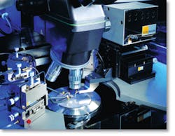
Figure 1. Pressure Testing to 100 psi
With the creation of microelectromechanical system (MEMS) devices using semiconductor technology, it could easily be assumed that standard testing methods and equipment also would be used. Unfortunately, this is not always the case.
While acceptable for static testing of MEMS devices, these systems only are suitable for determining the electrical characteristics and do not address the mechanical features or functions that also need to be analyzed. Dynamic testing of these devices requires other solutions for nonelectrical stimulation or measurement.
To meet these needs, a new generation of test equipment had to be created. These systems allow stimulation or measurement using sound, light, pressure, motion, or even fluidics. In addition, these tests often must take place in an environment that simulates the harsh environment these devices eventually will be used in: High or low temperature, pressure, and humidity or a combination of these may be required.
Some devices such as inertial sensors eventually will be in a controlled-environment package, and this also must be simulated for successful wafer-level test. Some devices, such as IR sensors, require extremely cold environments to minimize dark current for successful test and characterization.
Maintaining the required precision to contact the DUT while under these rigorous test conditions has proved challenging but not impossible. Most importantly, probing software, interfaces to equipment, and test software had to be created to use the same methodology that standard IC test platforms use. This has proved important in personnel training, accelerating time to market, and interpreting and correlating the test results when comparing wafer-level to final-product test.
Applying Pressure
Certain MEMS devices require pressure stimulation for test, and this application has necessitated the development of three unique solutions based upon the pressure levels required for the individual test. Solutions for both absolute and differential pressure applications are available.
For low-level pressure test (below 1 bar), a pressure chuck holds the wafer using vacuum on the outer edges, and pressure is applied to the center of the chuck surface. In this application, the membrane of the MEMS detector must be open to the backside of the device, and pressures above 1 bar are not possible because the vacuum is not strong enough to hold the wafer.
From 1 bar to 7 bar, an impact pressure nozzle blows a stream of air or inert gas down on the DUT from a controlled height, inducing a known pressure on the membrane of the device (Figure 1). The height automatically is controlled via an edge sensor, and the system is calibrated so the margin of error is less than 1%.
Above 7 bar, a new solution is required. Devices designed for process control where high pressures must be accurately detected and measured require a system that subjects the entire wafer to these high pressures while maintaining a safe environment for the test engineering staff.
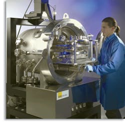
Figure 2. 750-psi High-Pressure Test Chamber
Using pressure-vessel technology from aerospace, high-pressure industrial processing systems, and nuclear submarine research, a semiautomatic MEMS probing system capable of subjecting the DUT to pressures as high as 50 bar (750 psi) has been developed (Figure 2).
Test Case 1: Testing Tire-Pressure Monitoring Systems
As a result of litigation that resulted from the Firestone/Ford SUV rollover controversy, the U.S. Congress enacted the Transportation Recall Enhancement, Accountability, and Documentation (TREAD) Act, requiring the use of tire-pressure monitoring systems (TPMS). The weight and cost-savings benefits of improved mileage and the elimination of spare tires make TPMS very attractive to the automotive industry.
Run-flat tires used with the TPMS can provide motorists with the ability to make it to a proper repair station. Run-flats have limited life once they have lost pressure. As a result, more than 40 million new pressure sensors will be required to satisfy market demand.
Testing these devices is accomplished using an impact pressure probe module. The probe station for this application has been designed for critical Z-height repeatability. Available in both heated and ambient systems, this impact stream completely covers the sensing membrane of the device. A controlled-loop feedback system ensures accuracy and repeatability of each test.
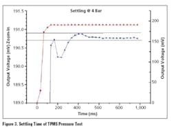
After a short stabilization settling time, the uniformity of the pressure applied to the sensor is stable and remains so for the entire duration of the test (Figure 3). Studies indicate near-perfect uniformity of the pressure across the entire surface of the membrane.
Simulating a Vacuum Package
Other MEMS devices such as inertial sensors have a different set of stimulation and environmental requirements. To perform at wafer level as they will when in their final vacuum package, these devices must be tested at a prescribed vacuum level.
The friction of air on the device structures makes free-air testing at wafer level impossible. To meet these requirements, a fully functional prober within a high vacuum chamber (up to 10-7 mbar) is used. Since a normal vacuum chuck is unsuitable for this type of chamber, a wafer carrier was designed which enables loading and mounts on the chuck that remains within the vacuum chamber.
The vacuum level is set by the test engineer. Once the desired vacuum level is achieved, the wafer is stepped device by device and tested. Both static and dynamic tests may be done on these devices.
Measurement of changes in the capacitance of the device when biased may indicate it is working and will allow engineers to compare these results to known-good die responses. While moving the MEMS structure, the movement may be measured using 3-D motion-analysis systems.
Resonators currently in development often require laser trimming while the device is being measured at high frequencies. This is challenging due to the high profile of typical high-frequency probes and the short working distance of the objective required for precision laser work. A multilevel observation port has been created in the vacuum prober to allow simultaneous alignment of the probes and trimming with the laser using high-power short-working-distance objectives.
Simulating Acceleration
An acceleration chuck allows measurement of the accelerometer in response to Z-axis motion on the chuck. One of the critical aspects of this system is maintaining contact with the DUT while it is moving and doing so without damaging the delicate pad structure that may be used later to connect the device to the final package. While design-qualification studies have shown little or no damage to pad structures after testing for extended periods, separate test and interconnect pads should be included in the MEMS design if real estate on the device is sufficient.
Test Case 2: Testing Inertial Sensors
Testing inertial sensors at wafer level often requires test within a vacuum environment to eliminate the friction effects of air on device components. One method stimulates the device electrically, and then movement is detected and measured. This testing confirms that the structures within the device are free and moving as designed. For full-functional test, these devices must be stimulated by motion, and the electrical signal generated by the device must be measured.
Special probes maintain contact while the DUT is moving. To understand these effects, a study was undertaken to look at the contact resistance over a 15+ minute period. The normal test time for the DUT is approximately 5 seconds while being subjected to 5g at 1 kHz. Contact resistance remained stable. To overcome potential probe bounce, an overtravel of 125 �m is used. Bond-wire pull testing on devices subjected to extended test time confirms that pad damage is minimal and does not affect final package yield.
Testing Microphones
Sound is used to stimulate MEMS devices when testing silicon microphones at wafer level. Shielding is required to protect the DUT from the outside noise generated in the prober and surrounding room. As in most MEMS wafer-level audio testing, a closed-loop feedback system that uses a reference microphone near the DUT monitors the stimulation at the test site (Figure 4).
Figure 4. MEMS Audio Testing Showing Reference Microphone
If the design of the device requires access from both the back and front side of the wafer for test purposes, double-side probing technology can be implemented. One European Si microphone manufacturer required electrical contact from the topside and sound stimulation from below. A noise box was used to generate the sound while remaining in contact with the wafer. SUSS programmable manipulators controlled movement of the sound box while the prober stage moved upward for die stepping.
Using Radiation Sources During Probing
Many of the sensors created using MEMS technology require controlled environments for test such as vacuum or cryogenics. These devices often must be exposed to blackbody radiation sources that accurately characterize the response of the device.
In some cases, arrays are characterized pixel by pixel to ensure uniformity. Care must be taken to guarantee that the device sees only the radiation source and is not blocked from this exposure by test-system components.
Case 3: Testing Microbolometers
Microbolometers are increasingly used as IR sensing devices in both cooled and uncooled applications. Due to their capability to operate at room temperature, they are a cost-effective alternative to the more expensive cooled devices.
The testing and characterization of these devices require a vacuum environment and typically involve exposing the device to a blackbody radiation source at a known temperature. A large observation window directly above the DUT allows exposure to the IR blackbody radiation source.
IR sources at different temperatures are closely positioned above the device for characterization, and the system switches from one source to another on command from the control system. High-speed production test is accomplished using a vacuum prober to step from die to die on the wafer.
Conclusion
Testing MEMS devices at wafer level can be accomplished and may save substantial money by not sending bad die through expensive packaging and packaging test. The testing of these devices requires MEMS-specific test strategies, equipment, and designs. Bringing in your test partners and vendors at the earliest possible date will save both time and money.
About the Authors
Don Feuerstein is the national sales and marketing manager at SUSS MicroTec and a leading contributor to furthering MEMS test technology within the industry. He has been involved in the semiconductor industry for more than 12 years. Mr. Feuerstein, a published author, performed undergraduate work at North Eastern University and earned an M.B.A. at the University of New Haven. SUSS MicroTec, 228 Suss Dr., Waterbury Center, VT 05677, 203-264-8397, e-mail:[email protected]Frank Michael Werner joined SUSS in 1999 and was responsible for the development of vacuum and cryogenic probe systems before becoming the business manager for optoelectronic and MEMS test systems. Previously, he held several senior R&D and design positions in companies such as Elektromat and CONVAC before joining Fairchild Technologies as head of R&D. Mr. Werner graduated from the Dresden Technical University in 1976. e-mail:[email protected]
FOR MORE INFORMATION
on MEMS testing
www.rsleads.com/409ee-222
September 2004
