Follow a real product through MIL-STD-810E testing to see how reliability growth contributes to a successful design.
Despite the continuing push for commercial off the shelf (COTS) items, many products still are designed from their inception to be flight qualified. When the intended platform is a fighter aircraft, the environmental tests are understandably harsh.
MIL-STD-810E, one of many standards that apply to products destined for defense use, stipulates the environmental conditions that a product must withstand to be qualified for a particular mobile platform, whether it is vehicular, shipboard, or aircraft.
Environmental tests include altitude, humidity, temperature, vibration, shock, and fungi. The intention of applying these tests is to prove suitability for use on the military platform.
MIL-STD-810E, however, never was intended as an indicator of product reliability, and the tests may not identify marginal design weaknesses that will show up later. Failure during field trials is expensive since system-proving exercises often cost tens or even hundreds of thousands of dollars to conduct.
For that reason, the reliability growth test methodology was introduced in the 1960s to address system reliability. A pre-production activity, it is a formal method of improving the design of the first article in a production schedule by intentionally overstressing the product to induce failures. The failure is analyzed, the design amended, and the product retested to ensure the same failure does not recur.
This process is repeated continually until a predetermined time has elapsed with no failures. Prime contractors that use this tried-and-tested methodology trickle it down to subcontractors by making it a contractual requirement.
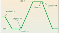
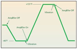
The most common test applied during reliability growth is random vibration combined with temperature cycling. A typical test cycle is shown in Figure 1. The product is non-operational during the ambient temperature ramp-down and remains off during the -40 F plateau. The plateau gives the internal circuits time to reach -40 F.
Figure 1. Reliability Growth Cycle
At the end of the plateau, the product is subjected to random vibration for a fixed period and then switched on while the ambient temperature is ramped up to +131 F. Again, the high-temperature plateau allows for temperature stabilization and the vibration reapplied. The entire cycle is repeated.
The Methodology in Action
The military needed a high-power C/D band microwave amplifier that could be mounted under the wing of a fighter aircraft inside a standard munitions pod. The RF performance previously was available in the form of a solid-state 250-W commercial product. The challenge was to reconfigure this amplifier to fit within the space and weight constraints of the pod while simultaneously ruggedizing the design to suit the new environmental conditions.
In the amplifier, eight RF power modules sandwich the power combining module. The AC/DC power supply is housed at the rear of the sandwich assembly. Top and bottom plenum chambers contain the control circuit, the driver amplifier module, and prime-power conditioning circuits. High-speed fans push cool air through the front of the unit.
The initial approach was to identify high-risk component and mechanical arrangements and produce appropriate risk-mitigation measures. These were used as inputs when generating the internal design specifications. The risk-mitigation measures included the following:
• Active and Passive Components Upgrade: Where available commercial-grade components were replaced with military-grade components.
• Wiring Interconnections: PTFE insulated wire used system-wide. Long-run coaxial semirigid RF cables clamped every 6 inches with rubber-lined metal P clips.
• Through-Hole Components: Leads formed to ensure good mechanical and electrical integrity prior to soldering. Tin finish was reapplied to lead ends during soldering process.
• Internal Temperatures: All modules were fitted with self-adhesive temperature labels.
Note that PVC insulation as used in commercial product wiring is brittle at -20 F (-29 C) and, although component leads come pre-tinned, bare copper is exposed during lead forming and cropping. Bare copper will oxidize rapidly in humid conditions so the tinning must be reapplied. The temperature labels were fitted inside the modules to allow the maximum internal temperatures to be ascertained and recorded.
As a confidence measure, the power and driver RF modules were given an early test for resilience to vibration. At the test house, they were subjected to the harshest specified vibration in all three axes. For simplicity, the two modules were not powered up during the test, but each module's RF performance was recorded beforehand to allow a before and after comparison. This exercise led to the first failure.
First Failure: Internal Wire Connections
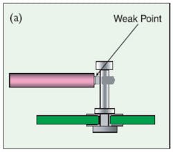
A post-test performance check and subsequent fault localization found that internal wire connections had failed in both modules. Investigation showed that an abrupt change in flexibility is formed at the point where solder stops wicking up the strands of multistranded wire.
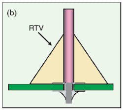
Figure 2a shows this weak point. All the failed interconnections had broken at this point. Reconnection of the wires showed the RF performance matched pre-test results. Inspection under a microscope did not indicate any other types of mechanical failure.
Figure 2: Stranded Wire Weak Point (a) and Solutions (b)
Prevention or severe damping of movement was required at the flexible/inflexible interface. The successful solution was to dispense with the solder terminal altogether, solder the wire directly into the PCB, and apply a cone of room-temperature vulcanizing (RTV) silicone rubber (Figure 2b).
RTV silicone is applied as a thick gel that self-cures in air. It is well suited because it has high tensile strength, good elongation percentage, and a peel strength of 20 lb/inch. It also has high dielectric strength, a brittle point of -100 F (-73 C), and a high temperature capability of +302 F (+150 C).
Prior to performing the reliability growth exercise, the amplifier was fully tested for compliance to the performance specifications. An immediate concern was whether the external connection cables such as RF feeds and prime power input would survive any whipping caused by the vibration test. This fear proved to be unfounded.
A common practice at environmental test houses is to arrange test cables in loose loops and secure the loops using Gaffer tape. Gaffer tape is a cotton-backed adhesive tape capable of withstanding wide temperature extremes. The name comes from its extensive use by lighting crews in the movie and stage industries.
Second Failure: High-Power RF Transistors
On the first reliability growth cycle, the RF output power dropped significantly at the start of the high-temperature plateau. Investigation showed that high-power output transistors in one module had failed.
High-power RF transistors have metal flanges screwed directly to the chassis floor. When the failed transistors were removed, a thin brown film was observed under the site of the flange.
A check showed that over-enthusiastic application of thread-locking fluid was used on this particular module. Thread-locking fluid has the capability to fill tiny gaps through capillary action and then set to a solid plastic of known shear strength. Excess application on the fixing screws allowed the fluid to wick under the device flanges before the device was fully tightened down. The devices then failed through excess junction temperature.
Although inspection showed no other flanges had film to the extent in this one module, use of the fluid on any device with integral heat sink was discontinued, primarily because of the inability to tell how much, if any, fluid had wicked under a flange. Spring washers were used as the only locking mechanism for these devices. This locking arrangement proved entirely suitable.
Third Failure: High-Power Transistor Connections
In the second session, the amplifier failed after completing five full cycles. The observed failure was no RF power output when switched on at the end of the low-temperature plateau. The cause proved difficult to find because the symptom did not show up at the factory.
Fault localization took several days of systematically applying freezer spray to small, localized areas. The fault eventually was located in the AC/DC power supply module a break in the connections between a high-power transistor and its PCB pads.
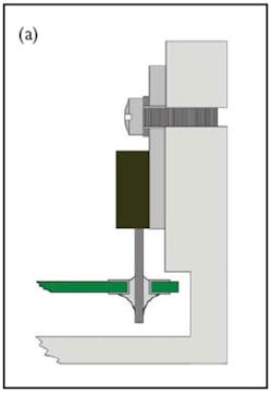
Figure 3a shows the TO220-package mounting arrangement. A fixing screw with a locking washer is used to fasten the transistor heat sink rigidly to the chassis wall. The leads are soldered on both the component and solder sides of the board. For clarity, the leads are not shown formed, and the irregular edges indicate the PCB continues on in that direction.
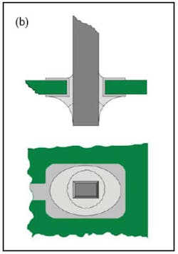
Figure 3: TO220 Mounting Arrangement (a) and Solder-Joint Failure (b)
Figure 3b is a sketch of the failure site. The fault shows as a faint annular ring approximately half way up the solder fillet on the solder side of the PCB. A microscope was required to see the ring clearly.
Disassembly showed the component leads could be pushed through the PCB. Inspection with a microscope indicated the cylinders of the plated through-holes were intact and still attached to their top and bottom pads.
The device heat sink is fastened rigidly to the chassis wall. Although fastened to the chassis floor in many places, the fiberglass PCB is comparatively flexible. It was concluded that vibration and different thermal coefficients of expansion induced high mechanical stress at the solder joint. Repeated stress application led to metal fatigue, resulting in simultaneous fracture of the solder fillet and shearing of the metallurgical bond on the long faces of the component leads.
Several options were considered to prevent or reduce the stress at the solder joint, most involving an improved fastening method for the PCB or placing some sort of kink or bend in the leads. The solution finally selected was a flexible connection based heavily on the stranded PTFE wire/RTV cone approach.
PTFE wires were connected from the PCB to the device leads, and RTV damping was applied to both ends of the wire, as shown in Figure 2b. For the device lead connections, the leads were offset from one another and 360-degree wire wraps made. The connections were soldered and a large single application of RTV anchored all three connections to the body of the device. This allowed relative movement between the device leads and the PCB without applying stress to the solder joints. Repeated tests confirmed the success of this arrangement.
Fourth Failure: Cracked Surface-Mount Components
The fourth failure was found while investigating the third failure. Microscopic examination discovered cracked surface-mount capacitors on the power supply PCB. The function of the components was not critical to the overall performance of the power supply module so only visual examination could identify the failure.
Typically, 1206 case style devices were soldered using a pointed tool to hold the component down. One side was soldered and then the other while maintaining downward pressure with the tool. Unfortunately, the second solder joint could be made with the component under stress. Although not critical in benign environments, the stress applied during reliability growth caused the component to fracture.
The solution: catch both solder joints briefly and then revisit the joints with fresh solder to relax the component. No further failures of this nature occurred.
Fifth Failure: External Screws
After five cycles in the third session, visual observation showed that two front-panel fixing screws were missing. An investigation revealed that an assembly step was missed when the amplifier was rebuilt.
Front-panel fixing screws are treated with breakable thread-locking fluid and torqued to the specified tightness. The thread-locking fluid step was missed during this particular rebuild, and some of the screws had shaken loose.
An at-a-glance indication that the fluid had been applied was required. As a result, a work instruction was initiated stating that red epoxy marker paint must be applied to the screw head to mark the status of the fixing screw. The paint bridges across the screw head and adjacent panel metalwork and acts as a tamperproof marker. The drawing package top assembly showed the marker paint locations.
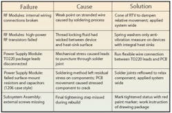
There were no failures during the fourth and final reliability growth session with the amplifier completing the prescribed time of 40 hours without failure. Table 1 is a summary of the failures and corrective actions.
The amplifier went on to complete all the MIL-STD-810E tests without failure. Besides the product sailing through MIL-STD-810E, the major benefits of the reliability growth exercise were increased confidence in the product design and increased quality since the revised assembly practices became commercial-grade practices. Although the reliability growth test methodology gives no guarantee of zero failures in the field, it significantly increases confidence in the design of a product.
About the Author
Thomas Mullineaux, the chief writer at HighTechWriter, is an RF engineer with 15 years experience in leading design teams. HighTechWriter, 3332 Florista St., Los Alamitos, CA 90720, 562-400-4501, e-mail: [email protected]
