Some expert advice can help sharpen your focus when buying an inspection system.
Buying an X-ray inspection system is a challenge and requires much research. There are many contradictory arguments that can justify every system from low-cost manual equipment where the operator does all the work and makes all the decisions to automated X-ray inspection (AXI) systems that sit in the middle of the production line and never need an operator.
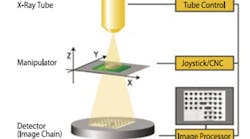
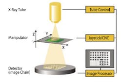
But no matter the bells and whistles a system has, such as automated movement, CT software, and automated measurements, it all starts with the general setup (Figure 1). The system consists of a microfocus or nanofocus� X-ray source; a manipulation or sample table, the dimensions of which determine geometric magnification, viewing angle, and sample size; and an image collection device such as an image intensifier or digital detector. While many of the components will have similar specs, how these pieces are assembled and in what combination greatly affect the image that is shown on the system screen.
Figure 1. Diagram of X-Ray System Setup
The Source
As shown in Figure 1, X-ray imaging starts with the X-ray source. For the great majority of PCB, IC, and other electronic inspection systems, the source is either a microfocus or nanofocus tube or a tube that will produce both. These tubes range in power from 50 to 225 keV, 50 to 500 �A.
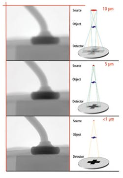
Microfocus tubes have focal spots of 10, 5, or 2 �m while nanofocus tubes can have focal spots of 500 nm. Image resolution or sharpness is determined principally by the focal-spot size of the X-ray tube and is approximately half the focal-spot size.
As a result, a nanofocus tube can resolve images as small as 250 nm while a 5-�m microfocus tube can resolve only 2.5 microns. This effect on resolution is shown in Figure 2.
Figure 2. Image Sharpness of a Gold Wire Ball Bond at Different Focal Spot Sizes
Beyond the focal spot, the tube�s voltage rating, specified in equivalent keV or kV, defines the penetrating power of the X-rays. The denser the sample, the higher the keV required to penetrate it. However, the higher the power, the wider the focal spot must be to prevent burn-through. For this reason, a nanofocus beam is not safely used above about 1 W while a microfocus beam can be used at the tube�s maximum power rating.
Tube current is measured in microamps or milliamps and represents the amount of electrons per unit time being emitted inside the tube to impinge onto the target. It is proportional to the X-ray intensity at a given voltage. The lower the intensity, the darker and more noisy the image and the harder to resolve defects. Image intensity also can be affected by the geometric magnification (GM) of the system.
GM = FDD/FOD
where: FOD = the focus object distance; the distance from the bottom of the
tube where the focal spot, that is the actual X-ray source, is
located to the test object
FDD = the focus detector distance, the distance from the tube to the
image detector
Increasing the FDD will cause the image intensity to drop by the square of the distance. A doubling of the FDD will cut the intensity by 75%.
While typical geometric magnification is limited to 1,000 to 2,500�, a combination of software, lenses, and cameras will zoom into images upward of 30,000� from the raw image. Caution should be used when seeing these higher numbers. Further magnifying an unsharp or badly resolved image will just give bigger pixels.
X-ray tubes also should be extremely stable with typical variations in emitted intensity of less than 0.5%. The lower the drift, the more consistent the results and the higher the system uptime.
The system also should be designed to limit the radiation exposure to avoid damaging sensitive ICs. As AMD1 has shown, some IC circuits can be damaged from as few as 5 Krads. For the typical silicon-based device, this is equivalent to a 40-minute exposure at 100 keV and 10 mA at FOD = 10 mm or 1.7 min at FOD = 2 mm. For that reason, look for tubes that have beryllium-free targets or systems with low dosing options to reduce the accumulated exposure to the components.
Sample Table
The sample table is the loading area for the devices that will be tested. The larger the inspection area, the higher the system costs. Systems range from sample sizes 8 inches � 8 inches to 28 inches � 28 inches with some semicustom units that can test a whole car. For PCB and IC package inspection, the sample must sit between the table and the X-ray source to minimize the FOD and maximize the magnification by keeping the source as close to the sample as possible.
The table also should be able to both tilt and rotate the sample in the X-Y plane. Tilting is accomplished by either moving the table up or down in the Z-axis or cantilevering the detector.
Many systems now offer up to 70� of movement, but a system with as little as 45� is common and useful. For high-resolution systems, the table construction should enable sample positioning at micrometer precision and avoid or damp any vibration that could diminish image sharpness.
Detector
The detector or real-time imager has seen the most improvements in the past few years as the industry ramps up for miniaturization, higher assembly complexity, and new interconnection techniques. The traditional image intensifier is an electro-optical device that amplifies and converts the invisible X-ray shadow to visible light by means of a scintillation crystal and photocathode. Electrons from the photocathode then are accelerated and focused onto a phosphor screen where a brightly visible image is produced and digitized by a CCD camera. The advantage of the image intensifier is its lower costs and sharp real-time image.
The new method is a digital detector made of CMOS, aSi, aSe, or CdTe. The X-ray shadow image still is converted by a scintillator foil to visible light, which then is directly detected by the photo diode array. While more expensive than the traditional image intensifier, this digital detector provides better, less distorted images with far superior contrast resolutions, an important feature for low-contrast applications such as adhesives inspection and where the board is populated on both sides.
Another consideration is whether the resultant image should be quickly acquired for higher throughput (2-D) or have slice-by-slice analysis for a more thorough inspection (3-D). To reduce inspection times, many 2-D X-ray inspection techniques use a fixed top-down view where the target board under examination is positioned between the source and detector.
The resolution of the image is determined by the size of the focal spot while the capability to resolve errors is affected by the magnification. Because of the top-down alignment, magnification typically is in the 200� to 400� range although some ultrahigh resolution systems offer up to 1,400�.
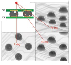
A variation of the 2-D X-ray is 2-D with oblique view at highest magnification (OVHM). These systems use an open-tube source that provides a high irradiation angle of 170� vs. approximately 38� for the narrow top-down topology for most 2-D systems. This maintains magnification during board tilting and rotation for complete inspection of BGA and other fine-pitch devices (Figure 3).
Figure 3. OVHM Capabilities Demonstrated for CSP Solder Joints
3-D imaging systems build on the 2-D X-ray with OVHM except both the X-ray source and detector move and the software engine captures multiple images to compile the 3-D image. This allows slice-by-slice analysis of the component, joint, or board but takes time to accumulate the image. In addition, 3-D system magnification typically is limited to 2� to 10�.
PCB Applications
For PCB inspection, the choice of an off-line manual or semi-automated system or an in-line AXI system is determined more by product type and volume. For large-volume cell phone or automobile modules that require 100% testing, an AXI system probably is the best choice.
For high mix, low volumes, or design verification, a semi-automated system with auto-decision software for more repeatable results is the better option. Complete manual systems, those without good software tools, are becoming less attractive except in applications with extremely limited budgets.
AXI systems have prices ranging from $500,000 to more than $1 million. Semi-automated systems range from $100,000 to $300,000, and manual systems typically are less than $100,000.
For boards with ball grid arrays (BGAs), top-down 2-D systems with a typical 120-keV tube will find bridges, missing joints, and misalignments. However, open solder joints normally require an inspection in 3-D or 2-D with OVHM to see a gap in the solder joint or an indication of insufficient wetting of the pad.
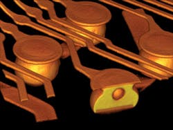
Smaller solder joints, such as in FBGAs, �BGA�, CSPs, and flip chips, must be tilted for accurate inspection. A system must use OVHM techniques to inspect these small joints and avoid indicating false positives. 3-D systems also can be a choice if test time is not a factor (Figure 4).
Test speeds can be improved significantly by selecting a system with a larger field of view (FOV). A large FOV allows a larger section of the board to be inspected in one acquisition. Combined with automated decision software, these systems can cut the inspection time on even large boards with many BGA or flip chip devices. Systems with large FOV have microfocus or combination microfocus/nanofocus tubes.
The large FOV is one of the main arguments against a nanofocus tube. In practical use, a large FOV checks gross errors such as misalignments, shorts, and major ball deformations. Close-up inspection of individual leads or balls and chips will benefit from the clearer image derived by a nanofocus tube.
For lead-free analysis, you might want to use the new high-contrast digital detectors. While these new high-resolution devices do provide better images, many customers have found little difference in contrast between the lead-free and eutectic tin-lead solders. However, alternative interconnections such as adhesives or solder joints concealed by strongly absorbing devices may require the contrast resolution of digital detectors.
IC Package Inspections
X-ray systems are used for back-end qualification and sample testing of IC packaging. Most applications are not in high-volume production but used more in failure analysis labs. In the past few years, most of the new systems have incorporated a nanofocus or combinational tube.
As shown in Figure 2, image resolution is the primary reason. As dies, bond wires, balls, and vias become smaller, the need for a higher resolution image becomes more crucial, making nanofocus a must.
These package inspection systems tend to be smaller machines with 8-inch sample tables. The tables also are easier to manipulate, providing upwards of 70� tilting. This lets you spin the DUT in multiple axes to fully inspect the package. Since image quality is crucial, OVHM techniques are a must for viewing vias.
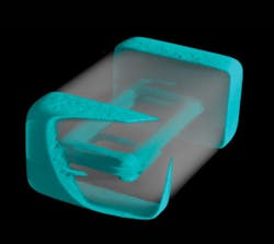
An alternative to the 2-D systems with OVHM is a 3-D system with sophisticated computer tomography or 3-D imaging techniques to create a slice-by-slice analysis of the IC. While a 3-D system tends to be more expensive than a 2-D system with OVHM, the details are much more dynamic, and analysis is down to minute details (Figure 5). New software also has reduced the time it takes to create a 3-D rendering of IC packages and other electronic devices.
Conclusion
With the many choices of X-ray systems available for electronic inspection, selecting the one machine that will be ideal for your application can be confusing. There are a plethora of inexpensive, manual inspection machines that fit the tight budgets many face today. At best, these inexpensive machines use 5-�m focal-spot tubes that limit the clarity of the image.
This means the operator must spend more time looking at the images to determine pass and fail results, which leads to more errors. However, they are the most affordable systems and will catch about 80% of the process errors.
Vendors of mid-range semi-automated systems, the standard for many years for PCB and IC inspection, have added more features, better tubes, and AXI-like controls and software. Features such as oblique views at highest magnification, 70� tilt, nanofocus tubes, and automated inspection software help keep this range of systems the leader in sales.
Prices creep up as the system becomes more automated. These systems tend to detect and correctly identify 99% of the assembly flaws in BGA and gull-wing components such as bridges, opens, missing joints, warpage, popcorning, component tilt, voids, and other shape deviations.
AXI systems also have shown improvements in testing and still are the only solution for high-volume inspection of automotive electronics and telecommunications devices that require 100% testing. From tilting up to 45�, higher resolution images, and faster test speeds, AXI has secured its position on the high-volume production floor.
Reference
1. AMD Publication # 26831 Revision A Ammendment/0, Aug. 19, 2002.
About the Authors
Dr. Holger Roth is senior applications engineer at phoenix|x-ray Systems + Services. He is in charge of the service lab for X-ray inspection and computed tomography. phoenix|x-ray Systems + Services GmbH, Kranstrasse 8, 70499 Stuttgart, Germany (011) 49 7 11.88 79 61-0, e-mail: [email protected]
David K. Lehmann is the West Coast vice president at phoenix|x-ray Systems + Services. He has nearly two decades of X-ray applications and sales experience. phoenix|x-ray Systems + Services, 111 Second Ave. NE, Suite 311, St. Petersburg, FL 33701, 661-242-1967, e-mail: [email protected]
April 2006
