Some helpful hints demystify the use of digital up and down conversion in today�s communications applications.
Digital up converters (DUCs) and digital down converters (DDCs) are not only critical in communications applications such as software-defined radio, but also can be helpful in applications where high-speed streaming of narrow bandwidth signals is required. In addition, the DDC architecture can be easily leveraged for alias-pro��tected decimation at all sample rates.
As an example, let�s examine the challenge of trying to digitally record a signal with 5-MHz bandwidth centered at 50 MHz. This signal could be an IF signal returned from an RF-to-IF analog down converter or a signal received directly from an antenna.
To simply meet the Nyquist criterion, we would need to sample this signal with a rate of 105 MS/s. However, to meaningfully capture this signal, we should sample at a higher rate of at least 200 MS/s. Assuming a 16-b analog-to-digital converter (ADC), a signal sampled at this rate generates 400 MB/s of data.
Perhaps even more daunting is the lack of commercially viable solutions to collect and store data at such high rates. Most available PC-based digitizers would only be able to store this data in portions of about 1 s.
Digital Down Conversion
DDC can digitally record an RF signal for an extended period of time. We only need to record the 5-MHz signal centered around 50 MHz, not the entire Nyquist bandwidth of the ADC. A DDC allows the rest of that data to be discarded and reduces the data rate. When performed in a field programmable gate array (FPGA), simple digital down conversion is broken up into three distinct steps: frequency shifting, filtering, and decimation (Figure 1).
Frequency Shifting and Filtering
The first step is frequency shifting. The 5-MHz band needs to be shifted down to baseband by multiplying or mixing the signal with a sinusoid at the carrier frequency (fc), which in this case is 50 MHz. The sinusoidal wave is created digitally using a numerically controlled oscillator (NCO). The NCO, also commonly referred to as the local oscillator (LO), can create a sampled waveform at a precise frequency and phase.
As the signal is frequency shifted from 50 MHz to baseband, a copy of the signal also is frequency shifted from 50 MHz to 100 MHz. For this reason, the new baseband signal has to be filtered to remove the upper frequency signals.
At this point, however, our task is not complete. We still have a low-frequency baseband signal that is sampled at 200 MS/s. Rather than overload the PC bus by transferring the extra unnecessary data, we resample the signal to reduce the effective sample rate. This is achieved by decimation where data points are removed from the digitized signal at regular intervals. In the example, to down sample from 200 MS/s to 10 MS/s, 19 samples are discarded for every 20 samples.
Alias-Protected Decimation
With decimation, the digitizer�s acquisition engine continues to sample at the same max rate. However, only a few of those points acquired are stored, fetched, and transferred to the PC, reducing the sample rate to the desired level. But, this technique is not foolproof.
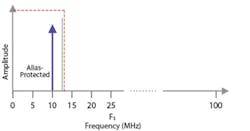
To illustrate, assume the digitizer�s maximum sample rate is 100 MS/s, which makes its Nyquist frequency 50 MHz, and the signal has two components: the fundamental at 10 MHz and a spur frequency component at 20 MHz. If the resolution of the digitizer is 14 bits, the total data rate at 100 MS/s is 200 MB/s, which is much higher than the PCI bus theoretical limit of 132 MB/s. This could be one of the reasons to use a lower sample rate such as 25 MS/s.
The Nyquist frequency now would be 12.5 MHz. However, the frequency component at 20 MHz aliases back to 5 MHz. Now, you can�t tell if the signal actually is a 5-MHz signal or another higher frequency signal (20 MHz, 30 MHz, 45 MHz) that has aliased to 5 MHz.
A solution to this problem is an enhanced decimation technique called alias-protected decimation. In this technique, the digitizer continues to acquire data at the maximum sample rate of 100 MS/s, but now a low-pass digital filter is applied with cutoff at Nyquist frequency before decimation (Figure 2).
Quadrature Digital Down Conversion
The DDC in Figure 1 only can be appropriately used with single-dimension modulated signals. An example of such a signal would be a dual-sideband amplitude-modulated signal for AM radio, which uses twice the bandwidth than actually is required. Such a signal is identical above and below the carrier frequency.
In Figure 3, the NCO produces two carrier signals: the I carrier and the Q carrier, which are phase shifted by 90�. These signals are independently mixed with the incoming IF signal to frequency shift it into its baseband I and Q components, and each path is filtered and decimated as before. From here, the I and Q signals can be further processed by the FPGA or recorded for processing later.
Figure 3. Block Diagram of a Quadrature DDC
Quadrature Digital Up Conversion
In the field of digital communications, signals need to be generated as often as they are acquired. Much like how a DDC was used to acquire an IF signal, a DUC is used to generate an IF signal. The DUC process is the exact inverse of the DDC process. Instead of down conversion and decimation, a DUC uses interpolation and up conversion.
Interpolation, or up sampling, translates a low sample rate modulated signal into a much higher sample rate signal that is ready for up conversion. This step, often performed in software, can multiply the overall waveform size by any factor. For example, you could interpolate a 16-kB modulated waveform to 32 MB with an interpolation factor of 2,048. Finally, the modulated, interpolated data mixes with a carrier that upconverts the baseband signal to the required carrier frequency.
An arbitrary waveform generator can download the entire up sampled, up converted signal to on-board memory. The generator with a DUC, however, performs the interpolation and up conversion stages in hardware instead of software, resulting in dramatically faster waveform computation and smaller waveform sizes. Expeditious processing and smaller waveforms save download time and enable longer playback time, which improve the statistical significance of many communications measurements and visualizations such as bit error rate, trellis plots, and constellation plots.
About the Authors
Kaustubh Wagle is a product manager in the modular instruments group at National Instruments. He has been with NI since 2003. Mr. Wagle received a B.S. in computer sciences and a B.A. in economics from the University of Texas at Austin. e-mail: [email protected]
Anuj Dharia, who has been with National Instruments since 2004, is a product marketing engineer in the modular instruments group. He graduated from Rice University with a B.S. in electrical engineering. e-mail: [email protected]
National Instruments, 11500 N. Mopac Expressway, Austin, TX 78759, 512-433-8000
May 2006


