Boundary scan is going crazy. From humble beginnings in 1990 targeted at solving the limited-access problems of traditional board test based on a physical-touch technology such as bed-of-nails and flying probe systems, IEEE 1149.1 boundary scan applications have expanded beyond the wildest imaginations of the original members of the Joint Test Action Group (JTAG).
We now have a plethora of related IEEE standards, 1149.4, 1149.6, 1532, and 5001, plus two major initiatives called IJTAG, now IEEE P1687, and SJTAG.
� IJTAG, I for internal, uses the test access port (TAP) as a major pathway into any form of test and debug instrumentation inside systems on a chip (SOCs) and similar devices.
� SJTAG, S for system, looks at the uses of a boundary scan infrastructure within a system composed of boundary scan-enabled boards and some form of backplane bus that can be used as a test bus.
As a result, boundary scan applications are expanding simultaneously in two completely opposite directions. But, does this mean that we finally have found the panacea for all the world�s test problems for electronic products?
The answer is no. There are some test problems that are very ably solved through a boundary scan approach and some that are not.
Where Are We Now?
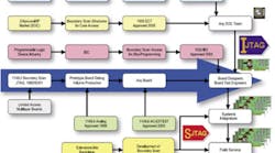
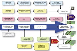
Figure 1 summarizes the explosive growth of boundary scan technology since the publication of the first version of IEEE 1149.1. Boundary scan has not only expanded at the single board level (1149.4, 1149.6, and 1532), but also has moved backward into core-based designs (1500, 5001, and now P1687/IJTAG) and forward into multiboard system designs�early multidrop architectures supported by various specialized scan-support chip sets now under further investigation by the SJTAG Working Group.
Figure 1. The Explosive Growth of Boundary Scan TechnologyECT: Embedded Core Test; ISC: In-System Configuration
Click here to see larger image
Does this mean that boundary scan solves all problems related to chip, board, and system tests? Before looking at this question, we need to define some common terms to prevent misunderstanding.
A device is defined as any electronic entity on a board. Once devices are assembled on a board, the board can be tested from a structural or functional perspective. Structural tests demonstrate conformance to the manufacturing specification, such as detection of faults introduced during the manufacturing process.
Faults can be device manufacturing defects such as gate-oxide shorts, metal-to-polysilicon shorts, metal trace bridges, open vias, seal leaks, dielectric breakdown, impurities, and bent/broken leads. Board manufacturing defects include missing devices, wrong devices, misoriented devices, opens and shorts in the bonding of devices to the board, track-to-track shorts, and open tracks. System manufacturing defects are incidences such as missing boards, wrong boards, boards inserted incorrectly in their sockets, and backplane interconnect opens and shorts.
Functional tests, on the other hand, demonstrate conformance to the design specification. Sometimes they are called design validation tests, especially in the world of device test.
One other major form of defects is categorized as wear out or environmental failures such as temperature-related, high-humidity, mechanical-vibration, electrical-stress, and radiation-induced errors. These faults are more devious to detect and diagnose and rarely detected by boundary scan techniques unless they manifest themselves as solid faults.
A boundary scan device is defined as any device that conforms to 1149.1, 1149.4, 1149.6, 1532, 5001, or 1500. Both 1149.4/6 and 1532 can be viewed as supersets of 1149.1 because they demand compliance to 1149.1 and then add extra features.
IEEE 5001 does not mandate compliance to 1149.1. But if a 5001 device is compliant to 1149.1, then use of the 1149.1 features to access microprocessor core debug ports is allowed. A 1500-compliant device also does not mandate 1149.1, but the core wrappers are based on the concept of a boundary scan register. Top-level control of the wrapper functions can be done through the 1149.1 TAP if it exists on the device.
Primarily, boundary scan can be viewed as an access mechanism to test and debug instrumentation inside devices or package pins and interconnects on a board. This access is via a primary test access port (PTAP), which, at the device level, is TDI, TDO, TMS, and TCK, the four mandatory signal pins of a boundary scan device.
At the single board level, the PTAP is the main entry/exit signal pins to boundary scan devices on the board; for example, the TDI, TDO, TMS, and TCK test points on an edge connector or header. At the multiboard or system level, the PTAP is the main access to boundary scan structures throughout the system; for example, a backplane test bus based on the 1149.1 protocol or some other bus protocol.
But not all devices are boundary scan devices. Multiple types of non-boundary scan devices exist that do not comply to any of the boundary scan standards; for example, a discrete device such as a resistor or capacitor, most analog devices, most memory devices, and power supply units.
However, on the board, some of these non-boundary scan devices will be accessible non-boundary scan devices, meaning that one or more of their signal I/O pins are directly accessible from one or more of the boundary scan devices on the board. Similarly, there also will be non-accessible non-boundary scan devices meaning that no signal I/O pin is directly accessible from any onboard boundary scan device.
What Problems Are Solved?
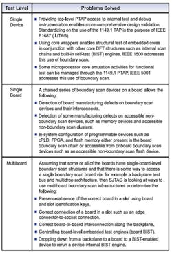
Table 1 summarizes the general class of test problems solved by boundary scan. Basically, it comes down to access and speed. Boundary scan and accessible non-boundary scan devices, in essence, can be touched via the boundary scan test registers lending themselves to test measurements.
Table 1. Test Problems Solved by Boundary Scan Techniques
But, boundary scan is inherently slow. Boundary scan devices typically work at TCK frequencies between 2 MHz and 60 MHz. Once a set of boundary scan devices is connected in a chain, the maximum frequency of TCK can only be as a fast as the slowest TCK in the chain.
Design-for-test (DFT) techniques, such as partitioning the chain into a number of shorter, separate chains, allow certain devices to be driven at higher frequencies. But, in the end, even a 60-MHz test rate will not allow any form of true at-speed testing. Consequently, the main defects caught by boundary scan techniques are those that result in permanent types of faulty behavior, such as stuck-at or stuck-together faults.
What Problems Are Not Solved?
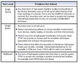
Basically, boundary scan cannot solve anything to do with functional test, be it low speed or high speed. Table 2 shows more detail.
Table 2. Test Problems Not Solved by Boundary Scan Techniques
Conclusion
Essentially, the problems solved by boundary scan technology relate to structural not functional defects. Even here, we rely on access to the target defects via the boundary scan wrappers at the core level and boundary scan registers at the single and multiboard levels.
No doubt, test engineers will continue to find innovative ways to use boundary scan infrastructures per the current IJTAG and SJTAG initiatives. But it is very unlikely that defects affecting high-speed operation of devices and boards will succumb to the charms of boundary scan.
References
IEEE 1149.1 Test-Access Port and Boundary Scan Architecture
IEEE 1149.4 Mixed-Signal Test Bus
IEEE 1149.6 Boundary Scan Testing of Advanced Digital Networks
IEEE 1500 Embedded Core Test
IEEE 1532 In-System Configuration of Programmable Devices
IEEE 5001 Global Embedded Processor Debug Interface Standard Rearick, J., Eklow, B., Posse, K., Crouch, A., and Bennetts, B., �IJTAG: A Step Toward a DFT Standard,� ITC 2005, International Test Conference Proceedings, paper 32.4.
�System JTAG: Supporting Embedded Boundary Scan Test,� SJTAG White Paper V1.0
About the Author
Dr. R. G. (Ben) Bennetts consults on product life-cycle DFT strategies and delivers onsite and open educational courses in chip and board DFT technologies. He is an advisory member of the Board of Directors of ASSET InterTech, a core member of the IJTAG and SJTAG initiatives, and the current chairman of the IEEE Board Test Technology Activities Committee, formerly known as the Board Test Action Group. 011 44 1489 581276, e-mail: [email protected]
FOR MORE INFORMATION
on IEEE 1149.1, 1149.4, 1149.6, 1500, 1532, and 5001
www.rsleads.com/605ee-177
May 2006
