Scan diagnosis is an established method for identifying and locating semiconductor defects on devices that fail manufacturing test and on field returns. Effectively selecting the right devices for failure analysis is a challenge. To address this challenge, some semiconductor manufacturers have incorporated scan diagnosis into the yield analysis process.
In a diagnosis-driven yield analysis flow, scan diagnosis is performed on a large number of the devices. Statistical analysis of the diagnosis results is used to identify the most probable cause of yield loss. Construction analysis then is performed on select devices to confirm the suspected root cause.
This flow eliminates the need for physical fault localization and in-
creases the failure analysis success rate. To enable a diagnosis-driven flow, advances in scan diagnosis techniques and proper analysis of the diagnosis results are required.
Overview of Scan Diagnosis
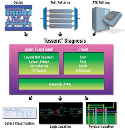
Scan diagnosis helps identify the location and classification of a defect based on the design description, test patterns used to detect the failure, and data from failing pins/cycles as shown in Figure 1. Scan diagnosis leverages existing design-for-test structures in the design and is based on automatic test pattern generation (ATPG) technology. Accordingly, scan diagnosis can only be used to diagnose ATPG or logic built-in self-test (BIST) patterns, not functional patterns. The output of a diagnosis tool typically is a list of suspects: the suspected locations and defect mechanisms for each defect on each failed die.
Figure 1. Typical Inputs and Outputs for a Scan Diagnosis Tool
Diagnosis results typically are measured in accuracy and resolution. A diagnosis result is accurate if the actual defect is in the suspect list generated by the tool. The resolution is determined by the number of suspects in the list provided by the tool and the physical area covered by these suspects.
One factor affecting the accuracy and resolution is the defect models used by the diagnosis tool. Traditionally, such tools would rely on the stuck-at fault model. If the actual defect did not behave as a stuck-at fault, the results could consist of a relatively large suspect list (low resolution) or a list that does not include the actual defect (poor accuracy). Despite these limitations, diagnosis has proven very useful in the failure analysis process.
Diagnosis Requirements for Yield Analysis
The accuracy and resolution of diagnosis tools have improved over time, enabling faster defect localization. However, when extending the use of diagnosis to another area such as yield analysis, you must look at the specific requirements for the particular application. Yield analysis typically is done to accelerate yield ramp, determine the cause of yield excursion, and improve mature yield.
A common goal in all these cases is to identify the root cause of yield loss. This process involves separating devices with systematic issues from those with random defects and then locating the physical defect. The separation process would be trivial if all devices with the same systematic defect exhibited the same failure signature.
However, the underlying cause is likely to manifest itself differently and in different locations for different die. Just looking at the failure data from the tester or even the location of the defect based on logic diagnosis is not enough to identify die failing due to the same mechanism. For instance, if a specific standard cell type has a problem that makes it more likely to fail, one instantiation of this cell may fail for one die and a different instantiation may fail for a different die.
To fully leverage diagnosis in the yield analysis process, the diagnosis tool must provide details that truly enable separation of die by:
• Defect mechanism such as interconnect bridge, open or stuck, cell-internal, at-speed.
• Physical location and features such as metal layers and vias in the suspect area.
• Logic location.
• Failing patterns, scan chains, and scan cells.
For diagnosis to be useful for yield analysis, we need an expanded set of capabilities compared to what is required for using diagnosis for failure analysis.
Expanding Diagnosis From Logic to Layout
Traditionally, scan diagnosis tools use the logic representation of the design. It is possible to expand the suspect classification. The challenge when doing this is to maintain high diagnosis resolution. Based on just a gate-level netlist, the best a tool can do is to look at which nets in the design would logically explain the failure. For instance, a certain failure may be logically explained by a bridge between nets A and B or a bridge between C and D.
In reality, nets C and D may be located far away from each other, and a bridge between these nets is not possible. Furthermore, it is impossible to differentiate between a bridge where only one net exhibits unexpected behavior and an open net.
This challenge represents the key motivation behind layout-aware diagnosis. In layout-aware diagnosis, a layout representation of the design is used in addition to the logic representation. This enables the tool to reduce the number of false suspects from the list by eliminating bridge pairs that are not within the line of sight.
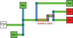
Layout-aware diagnosis also can reduce the suspect areas of open nets1 by analyzing the net topology. As an example, consider the multiple fan-out net in Figure 2. In this case, failures are observed on two of the five sinks of the net, which would imply the existence of an open somewhere on the net. By analyzing the net topology of the passing vs. the failing nets, the tool can narrow down the suspected defect area to the segment common for these two sinks.
Figure 2. Net Topology Analysis Example
The tool also can include the actual metal layers and vias that are part of this segment. This makes it possible, for instance, to identify a problem related to a specific type of via, even if different die have defects in very different locations.
Accordingly, layout-aware diagnosis is vital to yield analysis because it improves the diagnosis resolution and adds additional classifications needed for effective yield analysis.
Diagnosis Goes Deeper
At 90 nm and beyond, a significant number of manufacturing defects are inside the library cells themselves. This is caused, in part, by the increasing use of custom cells designed to deal with higher process variations.
The capability to differentiate between defects in the interconnect (backend defects) and those internal to the cells (front-end defects) is crucial to ensure that failure analysis can be performed in a timely fashion. It also provides useful cell statistics for yield analysis. This is achieved through cell-internal diagnosis, which enables faster defect localization for yield analysis and provides cell statistics for yield learning.2 Other areas in which diagnosis technology has improved include discovering defects that affect both the functional logic and scan chains (compound defects)3 and at-speed diagnosis.4
As a result of these improvements, a tool such as Tessent™ Diagnosis can diagnose defects down to a logic net and physical polygon, differentiate between defects internal to the cells and the interconnect, and classify a range of defect types.
Implementing a Diagnosis-Driven Yield Analysis Flow
Beyond the quality of results, there are other areas in which the diagnosis requirements are unique to yield analysis. When used for failure analysis, diagnosis typically is run on a very small number of devices. Tool runtime usually is not an issue, and it is acceptable to use dedicated patterns rather than production test patterns for diagnosis. In some cases, additional patterns based on the initial diagnosis results may be used to further increase the diagnosis resolution.
For yield analysis, the situation is different. In this case, diagnosis typically is done on hundreds or thousands of devices. This is required to perform sound statistical analysis. For that reason, diagnosis must be based on the production test patterns rather than dedicated test patterns to be effective. In addition to being compatible with traditional scan patterns, this implies that diagnosis must work in the presence of test-time reduction mechanisms such as scan test compression and logic BIST.
Furthermore, it is important that manufacturing test, data collection, and diagnosis are done in such a way that the impact on test and processing time is kept to a minimum. For instance, most semiconductor companies use a combination of stuck-at and at-speed test patterns.
A majority of defects may fail both of these pattern types, but diagnosing at-speed patterns typically is more time-consuming than diagnosing stuck-at patterns. Similarly, diagnosing scan-chain defects requires more fail data and more processing time than diagnosing failures in the functional circuitry. One particular defect mechanism may manifest itself as chain failures in some devices and logic failures in others. Even if the chain failures are ignored, the defect mechanism still can be identified.
While diagnosis results typically improve based on the amount of fail data used, research shows that diagnosis remains accurate even with a relatively small amount of fail data such as 256 cycles per die.5 By optimizing the test flow for diagnosis, the impact on test cost and overall resource requirements can be minimized.
Leveraging Diagnosis Results to Improve Yield
Diagnosis capabilities enable a volume scan diagnosis flow and provide detailed information about the failing die. To benefit from this information in yield analysis, we must properly interpret these results. We need to understand which devices fail due to systematic issues vs. random issues, to know what the systematic issues are, and then to select devices that best represent these systematic issues for failure analysis. Separating devices into different categories is particularly challenging when multiple systematic issues exist.
Wafer maps are one of the most useful tools for visualizing defect distribution across a wafer. By looking at a stacked wafer map, you can easily see if the majority of the failing devices is located in a specific location of the wafer or if one lot has a different defect distribution than another. Traditional wafer maps only indicate which devices fail, not why they fail.
The value of wafer maps can be extended by basing them on scan diagnosis results and normalizing the actual vs. expected data. For instance, a wafer map indicating all devices failing may show a random distribution of die across the wafer.
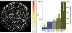
In Figure 3, a wafer map from the Tessent YieldInsight™ software tool shows failing die with a very specific signature: defects diagnosed to be an open where the diagnosed net segment includes single via4. The wafer is divided into multiple radial zones, allowing us to compare the amount of die with this particular type of defect in each zone.
As can be seen from the wafer maps, the concentration of die with this type of defect is highest in the outermost zone. This also is illustrated in the graph to the right. The thick bars show the number of die with defects that include single via4 for each zone. The narrow bars represent the expected number of failing devices. This expectation is based on the number of total defects in each zone and the percentage of failing die that include defects with single via4.
The expected number is different in each zone because the total number of failing die varies in each zone. In the outermost zone, the difference between the actual and expected number of die with this type of defect is statistically significant. The technique that automatically identifies the zonal type and the failure signature that has significant variance is called zonal analysis. It is one of several normalization techniques that can be used to identify systematic yield issues based on comparing actual vs. expected diagnosis results.
After a particular yield issue has been identified, the next step in the process is to select a small number of devices that best represent this issue for construction analysis, which will verify the suspected root cause. In the example in Figure 3, we would first select the 138 devices in the zone with the unexpected high concentration of defects including single via4. This selection can be filtered further by selecting devices with the best diagnosis results. This is done by choosing the devices with the smallest number of suspects. After selecting devices with a single suspect, you can choose the die in a similar fashion with the highest diagnosis score, which is where the tool has the highest confidence in the diagnosis result.
For the selected devices, you can use the combination of the specific diagnosis report, which would call out a net segment, similar to that shown in Figure 2, and the knowledge you gained from the statistical analysis, which in this example indicated a problem in single via4. As a result of this process, we know which devices to look at and exactly where in these devices to look—a cross-section of a specific via on that die.
When construction analysis, which is the physical inspection of the suspected defect, confirms the suspected cause, measures can be taken to correct the problem. This could be a change in the manufacturing process, containment by improving the test program to better target this specific mechanism, or a design change followed by a re-spin.
Conclusion
By combining highly accurate volume scan diagnosis with statistical analysis, engineers can implement a more efficient yield-analysis flow. Applying yield analysis based on volume scan diagnosis results that incorporate design layout and failure data rather than relying on manufacturing process data alone significantly reduces the time required to recognize yield issues and determine their root causes.
References
1. Keim, M, “Layout-Aware Diagnosis of IC Failures,” IC Design and Verification Journal, January 2009.
2. Sharma, M., Cheng, W.-T., Tail, T.-P., Cheng, Y.S., Hsu, W., Chen, L., Reddy, S.M., and Mann, A., “Faster Defect Localization in Nanometer Technology Based on Defective Cell Diagnosis,” 2007 IEEE International Test Conference, pp. 1-10.
3. Huang, Y., Hsu, W., Chen, Y.-S., Cheng, W.-T., Guo, R., and Mann, A., “Diagnose Compound Scan Chain and System Logic Defects,” 2007 IEEE International Test Conference, Paper 7.1.
4. Mehta, V. J., Marek-Sadowska, M., Tsai, K.-H., and Rajski, J., “Timing Defect Diagnosis in Presence of Crosstalk for Nanometer Technology,” 2006 International Test Conference, Paper 12.2.
5. Leininger, A., Muhmenthaler, P., Cheng, W.-T., Tamarapalli, N., Yang, W., and Tsai, K.-H., “Compression Mode Diagnosis Enables High-Volume Monitoring Diagnosis Flow,” 2005 IEEE International Test Conference, Paper 7.3.
About the Author
Geir Eide is a product marketing manager for Silicon Test Solutions at Mentor Graphics, where he also has been a development engineering manager and a technical marketing engineer. Previously, he held an applications management position at Teseda. Mr. Eide earned a B.S. and an M.S. in electrical and computer engineering from the University of California. Mentor Graphics, 8005 S.W. Boeckman Rd., Wilsonville, OR 97070, 503-685-7943, e-mail: [email protected]
March 2010


