Among the factors driving higher data rates, increased channel capacity, and superior noise immunity are limits in available RF spectrum, service in densely populated urban regions, and the need to provide efficient, long-range coverage for sparsely populated regions and developing countries. Creating components and systems capable of higher wireless data rates without compromise to power consumption or occupied bandwidth requires that special attention be paid to RF component and system design, characterization, and end-of-line testing.
Evolving high-order digital modulation schemes rely heavily on the successful detection of extremely subtle variations of the magnitude and phase, which creates very stringent requirements on each component in the signal chain from baseband to RF. The vector network analyzer (VNA) has always been used on the design bench due to its accuracy and flexibility, but to meet these requirements now is included in most validation and production-line testers.
The Right Tool for the Job
To correctly identify inadequacies in a wireless system or DUT, it is important to understand how individual components contribute to overall system performance. Wireless devices are made up of both linear and nonlinear components.
A linear component or a component operating within its linear range, by definition, does not introduce any additional frequency components to the RF signal. In other words, while both magnitude and phase are affected by a linear component, the same RF frequency content presented at the input will appear at the output, and no new frequency content will be present. Examples of typically linear components are filters and transmission lines.
Nonlinear components change the frequency behavior of a signal. While the input signal may be a single tone, the output signal of a nonlinear device could contain distortion in the form of harmonics or other spurs. Common components that will introduce nonlinear behavior to your device are power amplifiers and mixers. Also, when driven under certain conditions, linear devices exhibit nonlinear traits that are important to understand and account for in your design.
Several measurements are performed on wireless systems from absolute power on the simplest components to S-parameters and error vector magnitude on more complex combinations of components. A vector signal analyzer (VSA) typically consists of multiple mixing stages and a wide variety of filtering and signal-conditioning blocks to enable superior spectrum measurements over a broad range of frequencies. This architecture makes it suited for making nonlinear measurements, such as calculating the 1-dB compression point of an amplifier and identifying unwanted spurs in a mixer.
The more general-purpose architecture of the VSA can be replaced by the VNA when highly accurate phase and magnitude data are desired. The VNA is the preferred instrument when making linear measurements, such as the reflection and transmission coefficients of a filter or accurate phase and magnitude behavior over the frequency range of interest. Most often, your test bench will require a combination of these and other instruments, including signal sources, power supplies, digital I/O, and digital multimeters, each being chosen to make the measurements it is best suited to perform.
Architecture of a VNA
One of the most common uses of a VNA is to quantify the impedance mismatch between two components. As with any electromagnetic energy, each time an RF signal leaves one medium and enters another, a portion of that signal is reflected back.
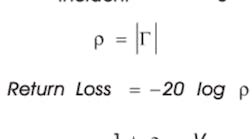
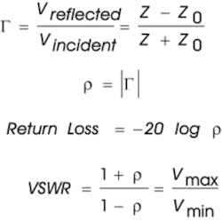
This reflection is caused by an impedance mismatch between the media or components and can be fully characterized by accurately measuring three signals: the signal at the input of the DUT, the reflected signal, and the signal at the output of the device. When each of these is measured as a vector quantity, you can calculate a number of key RF quantities including the complex and real reflection coefficients G and r, the voltage-standing-wave-ratio (VSWR), the impedance (Z), and return loss. The distinctive architecture of a VNA allows the separation of the transmitted and reflected signals to enable these measurements:
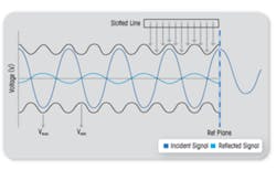
Figure 1. Standing Wave Resulting From Impedance Mismatch Between Components in RF Systems
Figure 1 illustrates how the superposition of the incident and reflected waves results in the constructive and destructive interference that forms a standing wave. The ratio of Vmax to Vmin of the standing wave is the VSWR caused by the mismatch. Prior to the advent of the VNA and the capability to fully separate and measure the incident and reflected and transmitted signals, a slotted line was used to accurately guide a probe along the line and make voltage measurements. From these position and voltage values, you can determine the Vmax and Vmin values necessary to solve for VSWR. Then using this information, the impedance and reflection coefficient quantities could be calculated.
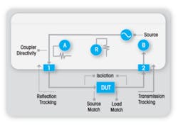
Figure 2 shows a simplified block diagram of the NI PXIe-5630 VNA, a two-port, one-path VNA. This simple architecture illustrates all the basic building blocks common to VNAs and responsible for their unique measurement capability.
Figure 2. Simplified Block Diagram of the NI PXIe-5630 VNA Showing Sources of Systematic Error That Can Be Corrected During a User Calibration
As shown in the figure, a stepped RF CW source is tuned through frequencies and power levels of interest. Directional couplers separate the incident signal from the reflected signal. In this way, the R or reference receiver measures only the signal produced by the source while the A receiver looks at only the reflected signal and the B receiver measures only the transmitted signal.
A wide range of IF BW settings allows you to optimize the test sequence for dynamic range or measurement time. In addition to the hardware architecture, a user calibration is always performed to correct for systematic sources of error within the VNA and test setup.
A user calibration is different from the periodic factory calibration completed by a certified calibration laboratory for all RF instruments. Factory calibrations typically are conducted yearly and ensure that the network analyzer meets the published specification. They also allow for adjustments to be made when damage or simple wear over time has altered the expected performance.
Even with the periodic factory calibration, the RF lab is a dynamic measurement environment and creates its own challenges, introducing both random and systematic errors. By definition, random sources of error are not repeatable or predictable. These random errors typically can be reduced by narrowing your IF bandwidth settings and averaging.
However, the key to the exceptional measurement accuracy achieved by network analyzers hinges on frequently performing a user calibration to reduce the systematic sources of error. Figure 2 shows the sources of systematic error that can be corrected for during a properly performed user calibration:
- Transmission and Reflection Tracking: Frequency response errors or transmitted and reflected signal loss result across all frequencies and must be characterized and corrected.
- Source and Load Mismatch: Many RF systems have a characteristic impedance of 50 ?. To properly measure the impedance of the DUT, any difference between this characteristic impedance and the impedance of the test port, or more specifically the reference plane, must be accounted for.
- Isolation: Errors can occur from crosstalk between various components in the test setup, VNA ports, and measurement reference planes. When this error is significant, it also should be included in your calibration procedure.
- Coupler Directivity: VNAs rely on directional elements, often couplers, to separate the transmitted signals from the reflected signals. Ideally, a directional coupler would measure only the forward or reverse traveling signals and produce an output for signals traveling in the opposite direction. Because this is never the reality, the error introduced by coupler leakage must be measured and corrected.
To correct for these systematic errors during a user calibration, you measure a set of known standards, compare the measured value to the value of the known standard to calculate the error for each data point, and finally apply the appropriate error correction for each frequency point in the measurement. This process is well defined for a number of calibration methods, and the correction factors and calibration coefficients are calculated and applied by the VNA.
There is a long list of well-defined, industry-standard calibration kits ranging from broadband short, open, load, through (SOLT) standards suitable for RF frequencies to transmit-reflect-line (TRL) kits when high accuracy over a narrow bandwidth is required. Additionally, automatic calibration modules are becoming increasingly popular, especially for automated network analysis in validation and production test where maintaining high throughput is so important and excessive time spent calibrating can be costly.
In addition to saving you time, automatic calibration kits extend the life of your expensive RF adapters and cables. All RF cables and adapters are rated for a limited number of connections. With an automatic calibration module, you perform only one connection during calibration rather than the five to 10 connections required for a comparable manual calibration.
Test Capabilities Enabled by VNAs
Extending the Reference Plane
In a VNA measurement, the reference plane is the location in the system where you performed the user calibration and consequently is the plane from which the measurement is being made. When calibrating a VNA using the SOLT method, for example, attaching the calibration standards to the ends of the cables connected to ports 1 and 2 establishes the end of those cables as your reference plane. Any adapters or a test fixture placed between those cables and your DUT are included as part of the measurement and can dramatically alter your results.
Consider a 6-GHz sine wave. With a 5-cm wavelength, even a single millimeter difference in your actual and desired reference plane results in 7.2 degrees of phase error. When testing semiconductor components and other RFICs, an industry-standard connector such as 2.92 mm or 3.5 mm cannot be used, and test fixtures are always used in some fashion to connect to the DUT.
The use of a test fixture makes it necessary to use some method of de-embedding to isolate the DUT from the test fixture or custom calibration standards that connect to the test fixture in the same way as the DUT. When it isn’t feasible to create custom calibration standards matching the test setup, VNAs are able to extend the reference plane of the measurement.
You can move your reference plane after calibration either automatically or manually by inserting an open or short calibration standard at the location in the test setup where you would like to relocate the reference plane.
Figure 3. Response of the DUT (Blue) Estimated (Yellow) by Using Time-Domain Gating to Remove the Additional Response of a Test Fixture (Green)
Figure 3 shows the full reflection that is measured by the VNA when the DUT is replaced by an open or short standard. The VNA then can perform the calculations necessary to move the reference plane and adjust subsequent measurements to match your desired measurement setup. For increased accuracy, you can use a VNA to characterize the test fixture and manually enter the values for trace length and frequency-specific loss. Then these are removed or added to your measurement to relocate your reference plane.
Time-Domain Analysis
Another function of VNAs is time-domain analysis. VNA time-domain analysis often is confused with the TDR functionality on an oscilloscope. The time-domain data available through a VNA can be thought of as addressing a superset of the problems that TDR can solve.
Where TDR uses a pulsed signal and a wideband oscilloscope to measure the reflection of that signal as a function of time, a VNA measures in the frequency domain and then performs an inverse FFT to give you the time-domain data. With a VNA, you will see high measurement certainty and higher resolution in the time domain, which is important when looking at a circuit with closely spaced components. You also can perform band-limited analysis rather than needing a DC path like a TDR oscilloscope requires. This becomes very important in production test when you want to reduce test times by limiting your frequency span.
Time-domain analysis is useful in making a distance-to-fault calculation. For example, time-domain analysis can locate a fault on your test board and provide information about whether the fault was an open, short, or some other impedance value. Time-domain data can be viewed in time and distance, which provides the location of the fault in addition to the electrical properties.
Time-domain analysis enables time-domain gating, another form of de-embedding that allows you to isolate and measure just one component in the circuit without recalibrating to extend your reference plane and isolate that component. By observing the varying impedance values through an RF signal chain, you can identify components in the system by time and distance.
Figure 3 shows that by gating only the desired components in the time domain and converting the data back to the frequency domain, you can estimate the magnitude and phase response of only the DUT and not the fixture or any additional adapters.
The Software-Defined Advantage
Where traditional instruments typically have a fixed software architecture with most of the functionality defined inside the box along with their own mechanical enclosure, processor, power supply, and display, software-defined instruments share the processor, chassis, power supply, and display across all instruments in a single PXI chassis. The test software resides on the host PC, allowing user-defined measurements and analysis in real time, a test setup optimized for high-throughput parallel testing.
Evolving Test Bench
As the demand on data rates and channel capacities continues to rise, precision RF components are essential to providing the high-quality signals required from baseband to RF. For their exceptional accuracy and flexibility, VNAs have become an indispensable tool on the design bench as well as in validation test systems and on the production line.
The hardware architecture enables you to precisely characterize the DUT. A VNA allows you to understand the electrical contribution that each component introduces. This facilitates design of wireless devices that keep pace with today’s demanding standards.
About the Author
David Broadbent is a product manager for RF and microwave test at National Instruments. He holds a bachelor’s degree in physics from Brigham Young University and is a member of the IEEE Microwave Theory and Techniques Society. Mr. Broadbent also participates in a number of industry conferences. National Instruments, 11500 N. Mopac Expwy., Austin, TX 78759, 512-683-6467, [email protected]
