What you’ll learn:
- The first CMOS chip was created by Fairchild Semiconductor, presented at ISSCC in 1963.
- The logic topologies used in today’s textbooks originated in this work.
- P-type devices are slower than N-type by about 2.5X because of mobility differences.
Planar bipolars
Took us to the moon and back
CMOS wins on space
On Wednesday, February 20, 1963, Frank Wanlass delivered a paper at ISSCC at U. Penn., written by him and his co-author C.T. Sah, describing Fairchild Semiconductor's process in which “N AND [their paper added this emphasis] P-type field-effect, metal-oxide-semiconductor-triodes [their paper’s italics] have been fabricated from silicon by a planar diffusion process.”
Much more so than the invention of the bipolar junction transistor in 1947 by Bardeen, Brattain, and Schockley (who left Bell Labs to found Fairchild...), Wanlass’ “CMOS” process would impact humanity in unforeseeable ways, perhaps providing the seed to its future extinction since it forms the basis of almost all ASICs in use today, including those powering AI.
What’s All This CMOS Stuff?
As a rabbit hole to go down, the one page of single column text in this paper is an interesting and quick read—watch me write more words about it than are in the paper, LOL. Wanlass & Sah provide figures:
- of the device cross sections of both the N and P type “elements,”
- which suggest symbols for the devices that don’t conform to present day usage (they have device-type arrows on the drain terminals instead of the source terminals),
- which show “characteristic curves for the field-effect triodes” as a four-quadrant plot, with the N-type in the first quadrant and the P-type element in the third quadrant. A 20-V swing in VGS would switch the devices’ IDS from 1 nA to 10 mA.
From this point, the authors dive into the use of these new devices for low-power logic circuits that only use the N and P elements, where they claimed that resistors and other components (TTL was in play at that time, as was Fairchild’s bipolar IC offering, which used bipolar transistors, diodes, resistors) were completely eliminated.
Perhaps this was a jab at Fairchild’s 1961 logic chip that was built using four transistors and five resistors, and the ensuing “Micrologic” family of 25 standard RTL devices (I almost said “RTL logic”). The latter would form the basis of a 5,000 NOR-gate (using metal-can uL903’s) designed by MIT and manufactured by Raytheon that became the Apollo space program’s onboard guidance computer for both the Command Module and the LEM. Our coverage of the IRE show’s logic IC announcements back in 1961 has been reprinted here.
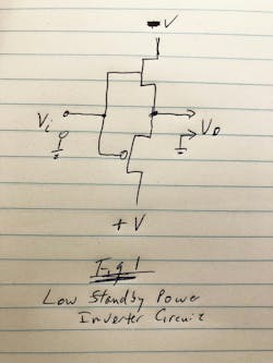
Each "triode,” as shown as in a logic inverter configuration in Figure 1 (the “bubbled” gate is the P device), would act as the other’s active load when the other device was switched off.
So, Vi set at −V would switch the P device on, turn the N device off, and connect Vo to +V. And, with Vi at +V, the N device would turn on, the P device would be off, and Vo would connect to –V.
Current only flowed during switching, with leakage in the off-device being the only current flowing in the circuit during its settled logic state—on the order of a nanoampere. Eerily, 62 years ago, these authors predicted that 107 inverter equivalent circuits (20M transistors) on a chip, perhaps seeming like an outrageous gate count at the time, would only dissipate 1 W.
A bit under two decades ago, we would produce our first 1B (109) transistor FPGA at Altera, using TSMC as our 40-nm foundry. It was one of the largest chips of its time and the first in the industry with an integrated 10-Gb/s, functioning, SerDes I/O. The only thing stopping them in 1963 was yield and lithography. Gordon Moore, who also worked at Fairchild in those times, set the cadence for the lithography heartbeat that fab-equipment makers lived and died by with his seminal paper.
A Triode Chain Has a Nice Ring to It
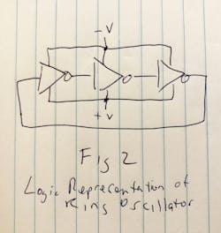
What to build in 1962 with planar, integrated P and N “triodes,” later known as “CMOS”? Having a low-power inverter, why not chain three of them together (Fig. 2) and make a ring oscillator out of the inverters of Figure 1? For copyright reasons, I can’t show the oscilloscope plot from their ISSCC paper, but the waveforms do show that the inverter propagation delays were less than 100 ns.
Interestingly, there’s a clear asymmetry between the waveform rise and fall times, as well as duty cycle, which its authors don’t address in the paper. Moreover, it does consistently seem to be about 2.5X slower for rise time than for fall time, which is explained by P devices having 2.5X less mobility than N devices. From this measurement data, we can infer that the first prototype inverters ever produced in a CMOS process by Fairchild had the same device width for their N and P devices!
Building symmetrical P- and N-type “triodes” probably made it easier for the layout techs. Mask generation back in those days involved cutting rubylith material by hand, taping it down (hence “tapeout” of chips), and then photographing the monster-scale artwork so that it could be shrunken down by projection to the 10-ish micron feature sizes of those days.
Three-Input NOR* Gate Minds Its Ps and Ns
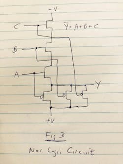
The paper then goes on to describe a three-input NOR* gate implementation using only the P- and N-type “triodes” (Fig. 3). It’s interesting to note that while our conventions have changed in schematics by having negative voltages at the bottom of a circuit, this diagram is identical* to the ones shown in modern day textbooks—and implemented in many ASIC process PDKs (which have “canned” logic gates for a given process invoked by higher-level circuit languages).
Operation is simple: The output Y can only be pulled low by the N devices if they’re all on, which means A, B, and C are at +V. With them all at +V, all of the P devices are turned off and not connected to the +V supply. NOR*. If any one of A, B, or C are low, Y can’t pull low to –V and one of the P devices connect the output to +V. NOR*.
One of the downfalls of these CMOS circuits is the asymmetry in mobility between P and N devices, which means that one will turn on or off slower than the other. Thus, during a switching transition, both P and N devices can be turned on, creating a dead short between +V and –V.
This is where Wanlass and Sah’s term of “active load” comes in—these devices have finite channel sizes and will act as resistors versus dead-short circuits. As a result, a complete sag of a finite impedance supply rail doesn’t occur, though minor sags or “glitches” in the supplies do occur during switching events in every CMOS gate to this day. In this regard, CMOS circuits are noisy and can affect sensitive adjacent circuits with poor CMRR and supply-noise rejection.
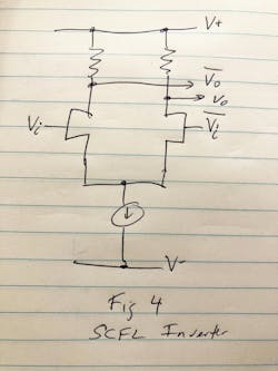
While we do see this problem of “shoot-through" in H-bridges and multiphase power inverters, logic gates don’t lend themselves to incorporating “dead time” in their switching cycles due to device count (which manifests as cost, power dissipation, degraded reliability, and lower manufacturing yield). The partial solution is to either perfectly match the P and N devices for rise/fall times, which reduces but doesn’t eliminate switching noise, or use differential logic, which pulls a constant current from a power supply and steers that constant current versus switching it on and off.
Figure 4 shows an example of such a differential logic inverter circuit.
If all goes to plan, we’ll try to do a SPICE simulation of a differential inverter circuit as both the next blog entry and as a Modeling on Mondays article.
All for now,
-AndyT
*[Editor's note: I blindly copied what was in the paper without thinking, which is embarrassing. An astute reader pointed out that this is actually a NAND function, not a NOR as the paper incorrectly calls it. So, including the diagram (Figure 3 is a faithful reproduction of what was in the paper, so I'm not asterisking it or its caption), please note that this is actually a NAND logic function that they implemented and discussed in the paper and while I go through the "all NMOS triodes must be high in series to make a low..." correctly, I call it what the paper did out of confirmation bias. It's NAND. Ugh!]
AndyT's Nonlinearities blog arrives the first and third Monday of every month. To make sure you don't miss the latest edition, new articles, or breaking news coverage, please subscribe to our Electronic Design Today newsletter.


