GaN FET technology solving audible challenges for high-performance audio amplifiers
By Ilian Bonov, GaN International Product Marketing Engineer, Nexperia
Gallium-nitride (GaN) FETs are becoming widely preferred in many products, from low power, low-cost applications such as smart device chargers all the way up to high power automotive applications. Mostly, designers are impressed by the increased efficiency and power density that GaN delivers, which results in devices that have greater power capabilities than their silicon counterparts. However, high-end audio amplifiers are also now increasingly turning to GaN technology as the smooth switching characteristics of GaN FETs result in less audible noise being injected into the amplifier.
Recently, big name manufacturers of audio equipment including Technics (Panasonic) have all announced new audio equipment that contains GaN technology. GaN FETs can switch faster than their counterparts with higher efficiency, therefore equipment size can be minimized. Recent high-end audio products, for example, are now switching at 400kHz, whereas previous generation amplifiers switched at 100kHz.
But for audiophiles, the ultimate goal is a pure sound. This means that any audible noise which may be fed into the amplifier should be kept to as close to zero as possible. Usually, higher switching frequency results in higher levels of EMI and higher levels of audible noise – exactly the opposite of what audio companies are trying to achieve.
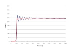
Yet the characteristic switching behaviour of GaN FETs is different to silicon devices. Figure 1 compares the switching waveform for a typical silicon MOSFET (blue line) used in previous generation high-end audio equipment and that of a GaN FET device (red line) that Nexperia manufactures and sells into the same application today. We can see that although the performance of the MOSFET is well suited to the task, there is a high degree of ringing at turn-off and that the peak voltage of 505V is much higher than for the GaN device. The GaN part is much smoother, with a peak of only 420V.
It should be noted that the silicon and the GaN devices are not exactly comparable, as they are different technologies, however, it is well established that the smooth switching that can be achieved with GaN FET devices results in significantly reduced noise – electrical and audible. A recent article in this publication, ‘GaN Transistor Eliminates EMC at Source’ by independent consultant engineer, Nigel Springett of Büro Springett (Bodo’s Power Systems, January 2021) presents measured data showing a significant reduction in EMI – 10dB at 170kHz – achieved primarily by replacing a silicon MOSFET with a Nexperia GAN FET in a 3kW power supply design. While the noise spectrum of that design is very different to the audible frequency, the principal is the same.
Why is GaN switching ‘smoother’ with less ringing than silicon? In Nexperia’s case, the answer lies in the design of the device.
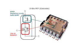
GaN HEMTs operate as a depletion mode FET with a naturally ‘on’ state. Most engineers prefer to work with naturally ‘off’ devices in switching applications due to safety and acceptability considerations. Currently there are two ways to deliver naturally “off” operation – single-chip enhancement mode (e-mode) or two-chip cascode mode devices. The gate structure of e-mode p-GaN HEMTs makes them very sensitive to gate drive voltage and they suffer from very low threshold voltages. They can also be difficult to drive. For these reasons, Nexperia prefers the stacked die cascode structure which pairs a low-voltage, low-RDS(on) MOSFET in series to the naturally ‘on’ GaN HEMT device (Figure 2). This configuration provides the robust and reliable insulated (dielectric) gate structure of a silicon gate, coupled with the improved voltage blocking characteristics of a high voltage GaN HEMT, effectively combining the benefits of the naturally ‘on’ operational state of a GaN HEMT with the safety and operational benefits of a naturally ‘off’ device. Even better is that the cascode device can be driven by standard cost-effective gate driver with simple 0-10 or 12 V drive voltage.
For the purposes of our discussion on noise – both audible for the high-performance audio amplifiers and EMI for the power supply example – the cascode structure offers additional benefits. Nexperia closely matches the capacitances of the low voltage silicon MOSFET and the GaN HEMT, with the silicon device acting like a filter, resulting in the smooth waveform. This capacitance matching is discussed in detail in a Nexperia paper entitled ‘Reliability and Performance Related to Internal Avalanche of GaN Cascode Devices’ by Yifeng Wu of Transphorm and Yan Lai from Nexperia.
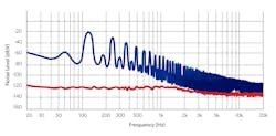
Switching power supplies have excellent instantaneous power supply capabilities and can achieve powerful sound, which are both attributes that suit high end audio applications. However, traditionally they have been viewed negatively because they generate noise due to switching operations. Higher switching speeds were also a problem for the same reason. Now, GaN switches with their smoother switching are enabling audio equipment manufacturers to rethink. Figure 3 is a representation of real data provided by one leading manufacturer which is now using GaN switches, and has increased the switching speed of its latest products to 400kHz – previous silicon-based amplifiers were limited to 100kHz.
The noise produced by the GaN power supplies in the new amplifiers (orange line) is considerably less than that of the older generation products (blue line) across the entire audible spectrum from 20Hz to 20kHz. The company employs a wide-band, low-noise reference voltage generation circuit and a control circuit in the new design. This ensures stable gain and achieves ultra-low noise characteristics that are flat down to low frequencies.
Summary
Nexperia’s industrialization of GaN has been extremely rapid. In the three years that Nexperia has been actively selling GaN devices, the company has moved from an initial launch position having 650V transistors with an RDS(on) of 50mΩ, to current devices which are rated at 35mΩ, and very shortly, 12mΩ parts will be available. Also, Nexperia – a leader on packaging technology - will shortly be offering GAN devices in CCPAK1212, a high-performance SMD package designed for GaN. Such devices bring obvious benefits of efficiency and power, but their smooth switching performance – optimized for efficiency – also means that they are an ideal solution for low noise applications too.
Readers can watch the GaN FET technology in action presentation and speak to experts at Nexperia’s online Power Live Event: 21 – 23 September www.nexperia.com/power-live


