Download this article in .PDF format
Op amps excel at providing many useful and clever solutions to routine or complicated circuit functions. A summing circuit is a perfect example. A summing circuit is typically used in applications where many inputs or channels need to be added or subtracted together to form a composite output. Combing multiple channels of audio is a perfect use for this circuit.
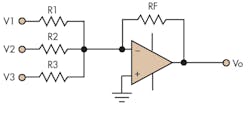
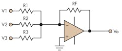
The traditional inverting op-amp summer configuration exploits the feature of a low impedance node (virtual ground) at the inverting input (Fig. 1).
The summing circuit is straightforward and easy to analyze and use, though it does have some limitations:
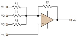
The summed voltages are all inverted. So what if you need to sum signals without inversion? Signals can be added without inversion by removing the ground from the non-inverting input of the op amp and then feeding a signal to the now available non-inverting input. A summing network can also be added to the non-inverting input, similar to that at the inverting input (Fig. 2).
Equation 2 is still manageable:
R1-R3 are interactive, but not terrible to deal with.
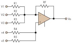
However, summing two or more inputs at the non-inverting input starts to get rather messy:
The non-inverting side of the equation reveals a large interaction with the other non-inverting summing networks in terms of voltage division, as well as the parallel combinations of the inverting input gain resistors, which makes the equation non-intuitive and difficult to use.
The process of calculating values in this circuit is iterative, interactive, tedious, and time consuming. This is one of the reasons why so many designers have shied away from using non-inverting inputs in their op-amp summer circuits. You could set up a spreadsheet to crunch the numbers, but that takes time. Even with a spreadsheet, looking at Equation 3, it’s still not easy to get a good intuitive handle on the non-inverting side of the equation.
There must be a better way. Many, many years ago when I was in college, I came across a very clever process for this type of circuit hidden in a chapter of Electronic Circuit Design by C.J. Savant. The technique in the textbook is credited to W. Philip Vrbancic.1 I also recently discovered that one of my colleagues at Analog Devices, Dan Sheingold,2 also developed his own very similar approach a few years prior to the Vrbancic derivation for solving this difficult problem.
The work shown here combines their works. I have always thought of their process as a very elegant solution and have never forgot it. The process is extremely intuitive and easy to use and allows for a variety of conditions, which can be solved in your head!
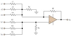
The full and detailed derivation of the design equations is beyond the scope of this article, but can be found in the references. Let’s look at the process in setting up this improved circuit. Figure 4 shows the technique used, which incorporates both non-inverting and inverting inputs and termination resistors. The design also minimizes the impact of offset error voltages at the output by providing equal and balanced input resistances.
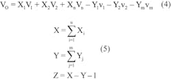
The addition of terminating resistors plays a large role in the ease of use of the circuit. Equations 4 and 5 express the general design equation for Figure 4, where the X terms are the non-inverting inputs and the Y are inverting input terms.
The lower-case variables in Equation 4 are associated with inputs that are summed at the inverting input of the op amp. The upper-case variables are associated with inputs summed at the non-inverting input. The X and Y terms are summed individually. The Z term indicates whether RX or RY is required in the circuit or neither is required.
The beauty of this design approach is its sheer simplicity. It eliminates cumbersome calculations and minimizes the user’s concern of interaction at the summing nodes of both the inverting and the non-inverting inputs. There are three different design constraints when using this technique.
Scenario I:
Scenario II:
Scenario III:
We’re almost ready to use the new circuit, but the value of the feedback resistor must be settled first. Similar to the above, there are three possible design approaches for designing these circuits:
• Design approach 1: Let RF = any number except zero.
• Design approach 2: Specify the minimum value for any resistor R connected to the input of the amplifier. For this case, we introduce the term Kmax. Let Kmax equal the greatest gain of any Xi, Yj input or Z. Then, RF = R(Kmax).
• Design approach 3: Neither input of the op amp should see a total resistance of no less than a specified value R. The term Kmax is equal to X or Y + 1, whichever is greater.
That’s it. With this information and the three design constraints and approaches, we’re ready to solve some normally very difficult problems. With this approach, they’re trivial. A few examples will help solidify the process and truly demonstrate how simple these circuits are with this technique.
Example 1
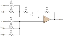
In this first example, design approach II is selected with R = 5 kΩ. Recall that design approach II specifies a minimum input resistor value. This design specifies that no values should be below 5K. The transfer function in Equation 9 shows the voltages to sum together for this example:
Vo = 5V1 + 7V2 + 2V3 – 2v1 – v2 [9]
Following the procedure discussed above, the non-inverting (X) and inverting (Y) terms are first summed together and then Z is determined.
X = 5 + 7 + 2 = 14
Y = 2 + 1 = 3
Z = 14 – 3 – 1 = 10 [10]
Recall from above that in design approach II, Kmax should equal the greatest gain of any Xi, Yj input or Z. In this case, the greatest number is Z = 10 = Kmax:
RF = R × (Kmax)
RF = 5 kΩ × (10) = 50 kΩ [11]
Since Z > 0 (scenario I), this circuit will require RY, but not RX. Now all that is required is to plug in the numbers. Recall from above:
Therefore:
The process is quite simple and quick to execute (Fig. 5).
Example 2
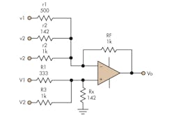
In this example we’ll use design approach I and set the feedback resistor this time to 1 kΩ. Therefore, RF = 1 kΩ. In this case we calculate X, Y and Z the same as in the first example, but we don’t use the term Kmax.In this example, the required output transfer function is:
Vo = 3V1 + V2 – 2v1 – 7v2 – v3 [14]
Therefore:
X = 3 + 1 = 4
Y = 2 + 7 + 1 = 10
Z = 4 – 10 – 1 = –7 [15]
Since Z < 0, this design will require RX:
Figure 6 shows the completed schematic.
Example 3
This last example uses design approach III, scenario III with R = 1 kΩ and an output voltage described by the transfer function:
Vo = 10V1 + 2V2 + 3V3 – 8v1 – 6v2
X = 10 + 2 + 3 = 15
Y = 8 + 6 = 14
Z = 15 – 14 – 1 = 0 [17]
Since Z = 0, this design will not use RX or RY. Calculate values:
Kmax = 15
RF = 1 kΩ × (15) = 15 kΩ [18]
The practical design approach presented here with the examples shown not only makes solving multiple-input op-amp summer circuits simple, it actually makes them fun to solve. This derivation is more intuitive, easier to use, and easier to understand than the first mentioned equations. It is scalable for a variety of inputs and is a truly elegant solution to a difficult problem.
References
1. W. Philip Vrbancic Jr., California State University, Long Beach, present at Wescon/82 Anaheim California, September 14-16, 1982.
2. Dan Sheingold, Analog Dialogue Vol. 10, No. 1 (1976), “Simple Rules for Choosing Resistor Values in Adder-Subtractor Circuits”
