Thermal Performance: Achieving Greater Power in Smaller Spaces
Members can download this article in PDF format.
Today’s designers are tasked with squeezing more and more circuitry into the footprint of their applications. The reasons are clear: smaller parts use less power, reduce running costs, extend battery life, and permit development of faster and smarter devices with greater functionality.
As a result, increasing power density and decreasing transistor dimensions have become hallmarks of contemporary ICs. Consequently, too, engineers often find themselves searching for a component that will fit in the space they have and stay cool while delivering the power needed for their system.
Sponsored Resources:
- Understanding power density: Increased thermal performance
- How to properly evaluate junction temperature with thermal metrics
- Understanding the trade-offs and technologies to increase power density
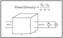
Shrinking systems and components leads to higher power density, which is a measure of how much power can be processed in a given space, quantifiable as the amount of power processed per unit of volume in units of watts per cubic meter (W/m3).
The ability to get the heat out of a semiconductor package directly impacts power density (Fig. 1). It’s best quantified by its thermal resistance, which is given by the temperature difference divided by input power. This has become increasingly important as packages continue to shrink, forcing engineers to look for new ways of optimizing thermal performance in space-constrained applications.
Thermal-Management Techniques
These benefits, however, also come with substantial challenges. Drawbacks start with the law-of-physics fact that shrinking systems and components results in higher temperatures. Why? Because larger-sized PCBs have more area for heat transfer to ambient air, thus reducing temperatures. Conducting layers within the PCB help spread the heat laterally, so adding more layers is beneficial.
If more layers aren’t possible, adding thermal vias at strategic locations can help. When multiple high-power-dissipating components are next to each other, it’s best to optimize their space for the lowest temperature rise.
Other useful techniques in thermal management include using low-resistance thermal-interface materials between two mating surfaces, applying gap-filler pads for large gaps, using heat pipes to transfer heat from hard-to-reach spots, using fans to create forced convection heat transfer, and employing cold plates to spread out heat.
Besides PCB improvements, a common technique to manage temperature rise is to use a heatsink attached to a component. Heatsinks are made of high-conductivity materials with significantly larger surface area for enhanced heat transfer with surrounding air.
Another option is to reduce the size of the power supply. Space-constrained applications often call for smaller power supplies. Such smaller power supplies, in turn, leave more room in a system for added functionality and processing power. But they can also trigger a tradeoff: Reducing power-supply solution size has traditionally come at the expense of reduced efficiency and thermal performance.
Simply shrinking a power supply usually means you will be dealing with a more challenging thermal scheme—it becomes harder to obtain a sufficient surface area in contact with air that’s necessary to achieve effective heat dissipation. And that means higher temperatures as power dissipation from components within the system causes their temperature to rise.
Similarly, as the trends progress toward miniaturization and cost reduction, the overall size of components such as the dc-dc converter also has shrunk. That means more attention must be paid to the junction temperature of semiconductor devices, which handle the conversion of power to a usable form. In addition, much effort has been spent on reducing the size of passive components used for energy conversion since inductors, capacitors, and transformers typically take up the largest portion of the solution size.
The primary factors limiting a designer’s ability to improve power density are converter power losses and the system’s thermal performance. Increasing the switching frequency can increase the power density, but there’s a good reason why power converters today typically switch no higher than the megahertz range: Increasing the switching frequency comes with the undesired side effect of causing increased switching losses and an associated temperature rise.
Get the Heat Out
As noted, a principal limiting factor to increasing overall power density is the thermal performance of the system. The ability to get the heat out of an integrated-circuit (IC) package directly impacts power density. The better the package is at removing the heat, the more power losses you can typically afford without seeing unreasonable temperature rises. Fortunately, a look around the industry shows that the necessary advances are happening.
Thermal parameters typically captured on datasheets include the junction-to-ambient thermal resistance (RΘJA), along with estimates of application conditions. Estimating junction temperature depends on the external reference point temperature and the thermal metrics of the package.
Commonly used package thermal metrics are the aforementioned RθJA and thermal characterization parameters. RθJA is a measure of the thermal performance of a semiconductor package. It’s not a characteristic of the package by itself, but of the package, PCB, and other factors. The junction temperature can be estimated with RθJA, although this may not be recommended unless the device is in a surface-mount (SMD) package.
The thermal characterization parameter Ψ, defined by JEDEC in the 1990s, is considered to be more suitable for estimating junction temperature in many cases. It represents the ratio of the temperature difference (between the junction and reference point) and the total dissipated power of the chip.
Aside from system thermal performance, power density can be held back by other limiting factors such as conduction, charge-related, reverse-recovery and turn-on/turn-off losses.
Packaging Solutions
Higher power levels in smaller form factors are now possible using TI’s advanced process, packaging, and circuit-design technologies. Let's start with packaging. Wafer chip-scale packaging (WCSP) is an attractive solution in mobile and space-constrained applications. Power is conducted directly from silicon to the PCB through a ball grid array (BGA).
TI is taking several different approaches to improve package thermal performance. For example, its power chip-scale packaging (PowerWCSP) focuses on thermal performance and current density optimization. PowerWCSP is an enhanced WCSP package capable of having a low package profile (maximum 0.3-mm thickness). Its unique bump structure improves thermal performance and current -arrying density compared to standard WCSP packages.
PowerWCSP takes advantage of the flexibility of copper post sizes to increase the area of key interconnects like power pins, without having to increase the die size or infringe upon the spacing tolerance of surface-mount manufacturing technologies. PowerWCSP solutions can run cooler compared to conventional WCSP designs.
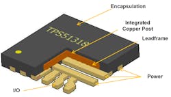
TI also has invested considerable resources in the development and adoption of the HotRod QFN package (Fig. 2), which replaces typical bond-wires while keeping a QFN-like footprint. A standard QFN package has wire-bonds connecting the silicon to the lead frame.
The company’s enhanced HotRod QFN with silicon die flipped directly on a lead frame utilizes low parasitic interconnects on silicon for reduced power dissipation, while still offering a large exposed pad for efficient heat transfer to the PCB through thermal vias. It brings together the best of both package technologies to optimize performance.
Conclusion
Achieving more power in smaller spaces and enhancing system functionality at reduced system costs are now possible using TI’s advanced process, packaging and circuit-design technologies. TI also offers design tools to help with product selection. These include WEBENCH Power Designer to design your power-supply circuit, and a PCB thermal calculator to understand the board area required for high-power dissipating components.
Sponsored Resources:


