Accelerate IC design with shift-left pattern matching
As the complexity of IC designs continues to grow, moving critical checks earlier in the design cycle helps designers identify and resolve issues before they escalate, streamlining the overall development timeline and improving product quality.
The shift-left electronic design automation (EDA) tools from Siemens EDA are transforming the way IC design teams approach physical verification. As part of the shift-left platform, the Calibre Pattern Matching tool helps to verify that the layout design matches the intent, debug issues quickly and accelerate towards a clean tape out.
Shift-left verification: Catching issues early with pattern matching
Many existing verification approaches rely on manual measurements and custom design rule checks that are time consuming to implement, data dependent and are conducted late in the design cycle. This means that critical issues related to symmetry, IP placement and other crucial design attributes may only be discovered after significant time and resources have already been invested, leading to costly design revisions.
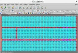
For example, today’s ICs integrate many IP from custom development and third-party vendors. While the IP providers deliver a clean layout, it’s ultimately up to you, the designer, to confirm that each IP placement is accurate and free of errors. Additionally, you must ensure the IP cells remain unchanged so they perform as specified and conform to guidelines. Figure 1 shows a layout with an IP row mismatch.
The shift-left approach with pattern matching
By moving critical pattern matching checks earlier in the design cycle, you can find and fix issues before they escalate, streamlining the overall development process. The key to this approach lies in the ability to leverage pattern-based solutions for accurate checks of symmetry, IP placement accuracy and other crucial design attributes as you work on the layout.
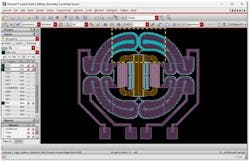
Verifying an intended symmetrical device is “click-button” easy. It can be done during device construction and repeatedly as the evolves, ensuring that the symmetry guarantee is maintained even as the block is placed within the context of a larger chip. Figure 2 shows a screen shot of interactive symmetry check in a design layout environment.
For designs with many integrated custom and third-party IP blocks, pattern matching solutions let you proactively check IP placements, ensuring that each block is correctly positioned and free from errors. Catching IP-related issues early mitigates the risk of late-stage functional problems and enhance the overall quality of the final product.
Streamlined debug
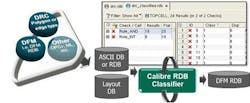
To prioritize and categorize errors more effectively, you can use the highly automated Calibre RDB Classifier to organize and manage verification data. As verification progresses, the RDB Classifier gives detailed insights into results, making it easier to understand error severity and focus on the most critical problems first. This streamlined debug process improves designer productivity, allowing you to quickly find and fix the root-cause issues, rather than sifting through large volumes of DRC violations. This organized, actionable feedback helps you make informed decisions and accelerate the path to tape-out. Figure 3 illustrates the RDB Classifier capabilities.
Improve efficiency, reduce time-to-market
Addressing critical layout issues early in the design cycle can significantly reduce the number of design iterations required, accelerating the path to tape-out. Moreover, the real-time feedback and streamlined debugging process with Calibre Pattern Matching lets you work more efficiently, focusing your efforts on the most pressing problems. This, in turn, translates to faster time-to-market and a competitive edge in the rapidly evolving semiconductor industry. Interactive, code-free verification use models allow designers to validate their work in real time without waiting on rule development or deck changes, further boosting productivity.
Embrace the future of IC verification
Shift-left Calibre Pattern Matching is at the forefront of the shift-left verification revolution, improving workflows, reducing unnecessary design iterations, and enhancing the overall quality of IC designs. As the complexity of integrated circuits continues to rise, the adoption of shift-left verification strategies powered by advanced pattern matching technology will be crucial for semiconductor companies looking to maintain a competitive edge and deliver high-quality products to market faster.
Figure 1. IP row mismatch error in a memory cell array. The middle ram block is missing matches along one word line (towards the left) where a modification resulted in a change to the bit cells.
Figure 2. Screenshot of Calibre interactive symmetry checking demonstrating how symmetry checking is conducted within the Cadence design environment using Calibre RealTime.
Figure 3. The results databases (RDB) hold a wealth of information for current and future design improvements. The Calibre RDB Classifier’s class IDs and duplication counts bring attention to results with the highest context repetition within the rule check.
This content is sponsored by:


