The growing Internet of Things (IoT) market continues to drive significant investment in new products, including smarter versions of existing products like the connected light bulb, or completely new products such as connected drones for videography, surveillance, and much more. Gartner expects 10 billion shipments of these types of products will flood the market by 2020; however, the market remains fragmented.
This file type includes high resolution graphics and schematics when applicable.
One common trend in this arena involves adoption of new techniques to lower power consumption of the principle ICs providing the intelligence for these systems. These techniques go beyond those used in today’s mobile, auto, and PC peripheral systems-on-chip (SoCs). The new levels of reduced power make it possible to fit into smaller spaces, shrink overall system cost, and increase overall battery life.
IoT Power Sources
The trend toward larger mobile-phone form factors enables the use of bigger, higher-capacity batteries, relieving some of the pressure on design teams to optimize the SoC for the lowest possible power consumption. The automotive market has the benefit of using a 12-V lead-acid battery as a power source, and USB-tethered devices are just that, tethered. Unfortunately, many IoT applications don’t have this luxury.
IoT applications are looking at either 25 years of battery life or very size-constrained spaces with limited room for batteries, while still meeting the expectation of adding elements such as wireless connectivity. So, while battery technology is slowly improving, minimization of the SoC’s power consumption as well as the system architecture will be the keys to making IoT designs “special.” For instance, a 570-mAh battery is estimated to keep Google Glass running for about a day, a 300-mAh source powers a Samsung smart watch for about two days, and a similar battery is good for up to 22 days when paired with a hearing aid.
Saving Energy in IoT Devices
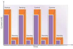
Figure 1 compares a typical energy use case for a generic IoT application, shown in orange, with the desired profile, shown in purple. The goal is to reduce the entire area under the rectangles. This requires both reducing the peak usage of each function (amount of real work) and the time required to perform the task.
It’s clear that IoT designs must go far beyond the advances made thus far by the mobile market to meet the power requirements of next-generation products. However, different applications require very different power use cases. Some use cases are dominated by “always on” functions, such as voice activation and power supplies. Others are off 99% of the time, such as motion, fire, and other environmental detection, which means a preponderance of standby power usage, whereas others are somewhere in between these two extremes. Each use case requires different considerations to minimize power.
If the device operates in such a way that dynamic power is the biggest contributor, an effective strategy is to reduce VDD as much as possible. If static power dominates, controlling the leakage per operation becomes more important.
New investments are already benefiting SoCs for IoT applications. For instance, IoT-specific process technologies developed by foundries support lower leakage and lower voltages, yet still meet processing performance demands.
On the design side, the mobile community and others have taken advantage of techniques such as clock and power gating, multi-voltage domains, dynamic voltage and frequency scaling (DVFS), and back-biasing. IoT teams are adding smart biasing, sub-threshold, and near-threshold design, and making more extensive use of multi-voltage, shutdown, and power domains, to accomplish very aggressive goals. Effective tools are required to ensure consistent interpretation of power intent, power network synthesis, and in-design rails, as well as deliver optimal low-VT usage and comprehensive power-aware formal and static verification.
Energy-Efficient IP for the IoT
Advances, innovations, and new investments beyond the mobile market in both process technologies and design techniques will absolutely drive new IoT products closer to reaching power-consumption goals. However, it will be differentiated IP and integrated IP subsystems developed specifically for IoT applications that will truly create viable, competitive SoCs.
Logic libraries, embedded memories, and non-volatile memories
In the mobile domain, low-power logic libraries and memory compilers are essential ingredients in producing efficient SoC implementations. In the IoT world, design teams supplement this with advanced low-power options, including always-on libraries, lower-voltage memories and libraries, multi-channel lengths, multi-bit flip-flops, and power-optimization kits. Ultra-low-power non-volatile memory (NVM) IP is being used to supplant more power-hungry options. ROMs now store mature code, beyond just boot functions such as USB and Bluetooth stacks, thus minimizing code storage costs and lowering power versus alternative options. A number of integrated test-and-repair solutions now support embedded flash to speed development, which increases test coverage, provides in-field diagnostics, and ultimately decreases costs
Efficient processor cores and IP subsystems
One of the most effective ways to reduce power usage is to shorten the time it takes to perform tasks. Using co-processors and dedicated hardware to perform specific functions will shrink the overall time.
Frequency and the amount of memory required to support functions also contribute heavily to power usage. In that regard, higher-performance processors and tightly integrated subsystems, in terms of the amount of work completed per cycle, can improve overall system and design costs. Co-processors, more efficient processors, and customized hardware will provide huge benefits by reducing frequency and memory requirements of functions such as voice, vision, motor control, power conversion, filtering, and audio.
Today, designers tackling IoT applications make more use of integrated IP subsystems that significantly reduce wait states within the architecture and optimize the overall die area needed to perform the tasks. For applications that require advanced math and very tight timing control, or must support “always-on” functions, improved processing capabilities (beyond just increasing frequency and pipelines) can dramatically enhance power consumption. Application-specific analog interfaces can also be used to manage functions for metering, medical, and power-management applications. They help better control the system and increase efficiency via higher resolution and higher conversion rates.
Interface IP
Standard interfaces designed for mobile and networking markets are being effectively used by IoT design teams, such as low-power RF solutions, DDR, MIPI for camera and display, Ethernet, and USB supporting battery charging and power-down features.
To further reduce peak current levels and task time, the industry is increasingly implementing new wake-up features, more flexible sleep modes, and interoperable low-bandwidth wireless radios that minimize the overall payload required to transmit.
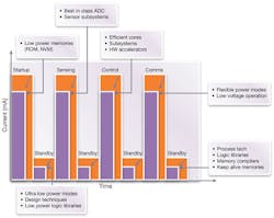
Figure 2 summarizes some key techniques for achieving lower power in specific IoT functions:
• Support boot loaders via ROMs, rather than fetching from traditional methods.
• Support options during startup to lengthen the time to load memory to reduce startup currents.
• Support of more flexible low-power modes ensures only the necessary SoC modules are operating, since this can change during the use case. For instance, during communication functions, sensing and measurement may not be feasible or desired and vice versa.
• During sensing and measurement stages, reduce the number of cycles and wait states. This is accomplished via improved analog measurement capabilities (higher resolution and/or higher conversion rates) and a reduced number of cycles to process the data (tightly coupling these interfaces with efficient and flexible processing cores in integrated subsystems). Processing can always be done by using a processor with a longer pipeline or increasing the frequency, but both of these options increase power consumption. Therefore, it’s best to use processors that complete the most work per cycle at the lowest frequency.
• Process complex math at minimum frequencies, in the least amount of time. When combined with enhanced sensing capabilities, this efficient processing reduces system mechanical costs on top of the PCB-related system savings. A good example is the implementation of vector-oriented control for motors, which has improved control and reduced the size of the motors over the past few decades. It should benefit new applications such as quad-copter drones, as well as traditional pumps found in appliances, utilities, and factories.
• Communicating at the proper time and with the appropriate amount of data payloads enables the application to right-size the power usage. This is being done with newly introduced low-bandwidth wireless standards.
• Employ the proper sleep states, with only the necessary “always-on” circuits, and minimize leakage with a low-power IP methodology.
Solving power issues isn’t the only driver for IoT applications. Design teams also face challenges such as increasing integration to lower system costs, adding connectivity and security, and simplifying supply costs, while improving ease of use, meeting tighter project schedules, and getting to market first.
Though IP requirements can vary greatly depending on the specific application, it’s clear that IoT design teams need low-power, robust, and proven IP solutions that help them achieve silicon success and quickly get their products to market.
Summary
The Internet of Things is spawning hundreds of new products and applications for wearable and machine-to-machine markets. These applications demand innovative design techniques, the use of established and advanced process technologies, and most importantly, innovative low- power IP to reduce power consumption and increase battery life.
This file type includes high resolution graphics and schematics when applicable.
In turn, many chip companies are exploring and/or investing in new business opportunities offered by the IoT market. However, these investments need to include the adoption of IP designed specifically to meet IoT application requirements. This will accelerate design development and get products to market faster, with significantly less risk. Risk management of SoC power usage is critical for IoT devices.
By adopting IP tailored specifically for IoT applications, design teams are able to reduce power, add connectivity, improve sensory and communications interfaces, and ultimately achieve design goals faster, with less risk.
Ron Lowman is the strategic marketing manager for IoT at Synopsys. Prior to joining Synopsys, he spent 16 years at Freescale, where he was most recently the industrial business development manager for the company’s Microcontroller Division as well as the product marketing manager for industrial MCUs and digital signal controllers. Ron holds a Bachelor’s of Science in Electrical Engineering from The Colorado School of Mines and a Master’s in Business Administration from the University of Texas in Austin.
About the Author
Ron Lowman
Strategic Marketing Manager for IoT
Ron Lowman is the strategic marketing manager for IoT at Synopsys. Prior to joining Synopsys, he spent 16 years at Freescale, where he was most recently the industrial business development manager for the company’s Microcontroller Division as well as the product marketing manager for industrial MCUs and digital signal controllers. Ron holds a Bachelor’s of Science in Electrical Engineering from The Colorado School of Mines and a Master’s in Business Administration from the University of Texas in Austin.


