What’s The Difference Between IGBTs And High-Voltage Power MOSFETs?
After evolving side by side over the past three decades, insulated gate bipolar transistors (IGBTs) and MOSFETs now dominate the power semiconductor market in applications such as motor drives, uninterruptible power supplies (UPS), and solar inverters. So where do IGBTs make the best fit, and when does it make better design sense to go with a MOSFET?
Related Articles
- Analyze MOSFET Parameter Shifts Near Maximum Operating Temperature
- Informed Analysis Picks Better 555 Timer To Drive Power MOSFET
- High-Voltage IGBTs Move Into Automotive Apps
Basic Structures And Principles
The IGBT is a semiconductor device that combines the output characteristics of a bipolar transistor and the gate drive characteristics of a MOSFET. So, the IGBT is a minority-carrier device with high input impedance and high current-carrying capability. Compared to MOSFETs, IGBTs also are better suited to scale in current handling capability at higher voltage levels due to their bipolar output characteristics.
This file type includes high resolution graphics and schematics when applicable.
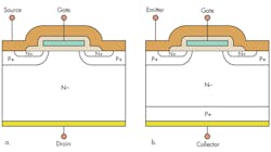
To turn on a typical planar high voltage N-Channel MOSFET, positive voltage must be applied to the gate with respect to source (see the figure). If the gate-source voltage is at or above the MOSFET’s threshold voltage, sufficient electrons accumulate under the gate to create an inversion layer, forming a conductive channel across the P+ body region. This enables current flow from drain to source (conventional flow; electronic flow is from source to drain).
To turn it off, the gate-to-source voltage is reduced below the threshold. (Practically, Vge is reduced to 0 V.) As a result, the inversion layer no longer remains, and the forward drain current flow is blocked. In the off state, the reverse biased body-drain p-n junction supports the drain-source voltage.
In N-channel MOSFETs, only electrons flow during forward conduction, and there are no minority carriers. Thus, the switching speed is limited only by the rate that charge is supplied or removed from the parasitic capacitances of the MOSFET. This is a key point to note and is the main reason why power MOSFETs are used when high switching speeds are essential for the end application.
One of the key performance-related characteristics of the MOSFET is its on resistance, RDS(on). In general, a conventional power MOSFET’s RDS(on) increases sharply with the breakdown voltage rating due to an increase in the thickness of the drift region required to support the high operating voltage. With the advent of super-junction MOSFETs, this has reduced the RDS(on) for the same breakdown voltage (made the relationship between RDS(on) and breakdown voltage rating relatively linear rather than a square law). Super-junction MOSFETs are thus increasingly utilized in applications where a low RDS(on), high blocking voltage, and fast switching speeds are needed to achieve high efficiency and power density such as in-server power supplies.
The operation of an IGBT is very similar to a power MOSFET in terms of creating an inversion layer by means of applying sufficient gate-emitter voltage. This flow of electrons draws positive charges (holes) from the p-type substrate into the drift region. This significant increase in conductivity of the drift layer enables a dramatic reduction in the on-state voltage of the IGBT.
This conductivity modulation mechanism enables the IGBT to achieve a higher current density and capability compared to that for a similar voltage rated MOSFET. During the turn-off, electron flow is stopped (as in a power MOSFET), yet holes remain in the drift region. These charges have to be removed by a recombination process. IGBTs, then, typically exhibit a tail current during turn-off until all the holes are swept out or recombined. Today, modern IGBTs are designed with a minimal tail-current effect.
The main advantages of an IGBT over a power MOSFET are the much lower on-state voltage drops due to conductivity modulation. This feature translates to a smaller chip size compared to that for a MOSFET for the same current and voltage ratings. The balance in tradeoffs between switching and conduction losses is being fine tuned so the line between IGBTs and MOSFETs is blurring in many applications. This leads us to the question of how these devices compare in a given application.
Application Perspective
Given the widespread availability of both IGBTs and high-voltage power MOSFETs with 500- to 800-V breakdown voltage ratings, designers often face the challenge of selecting either an IGBT or MOSFET for a given application and set of operating conditions.
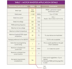
In the case of three-phase variable speed motor drives in the 300-W to 5-kW rated power range, utilizing a dc bus voltage in the 300- to 400-V range, and typically implemented by a six-switch inverter topology, 600- to 650-V rated IGBTs (co-packaged with an anti-parallel fast recovery diode) have traditionally been the preferred device from an overall performance perspective. But with the availability today of high switching speed, low RDS(on), and relatively fast recovery body diode 500- to 650-V rated power MOSFETs, it raises the question of whether it is time for the IGBT to give way to the MOSFET.
Focusing on performance considerations only, and with the aim to select a device that achieves the relatively lower loss in an example application’s conditions, we can compare example IGBTs and high-voltage power MOSFETs (Table 1).
For this purpose, simplified loss equations are implemented in Excel assuming a hard switched half-bridge topology. The simplified loss equations, the devices selected for comparison, and the assumptions made, along with the actual Excel calculator file, are available at http://am.renesas.com/products/discrete/igbt/Application_Notes.jsp.
Two representative TO247/TO3P packaged and closely matched (in terms of key electrical ratings) IGBT+FRD and MOSFET devices are selected for this analysis. Table 2 shows a snapshot of the calculator and results of the analysis.
Reviewing The Results
From the results of the exercise, the IGBT has the advantage over the MOSFET at higher switching frequencies. But at lower switching frequencies, the MOSFET has the lower overall loss and lower operating junction temperature. (The selected IGBT and MOSFETs have approximately the same die sizes and thermal impedances.)
This is in some ways counter to conventional wisdom where it is often argued that MOSFETs perform better at higher switching frequencies. However, these results indicate otherwise and can be attributed primarily due to the significantly lower diode recovery loss component of the IGBT+FRD (fast recovery diode) and the significant improvement in minimizing the tail current behavior of the IGBT.
The lower switching loss of the IGBT+FRD due to a significantly lower diode recovery loss component gives it the advantage over the MOSFET at 20 kHz (a relatively high switching frequency for this application).
Also, the MOSFET’s switching loss can be significantly reduced by use of a gate driver with a higher sourcing and sinking current capability (say a 2-A sourcing/sinking current rated driver). As a result, the overall MOSFET losses would reduce and would allow the MOSFET to close the gap between it and the IGBT. The resulting higher dv/dt, though, could cause undesirable effects such as high frequency ringing and a higher level of radiated EMI.
Interestingly, at lower switching frequencies where conduction loss dominates, the MOSFET benefits due to the lack of a “knee” in its forward characteristics, in conjunction with a relatively low RDS(on).
While the IGBT is still the better device to select in this application example, the availability of significantly lower RDS(on) MOSFETs along with improved diode recovery behavior and a strong gate driver could start tilting the balance towards the MOSFET. In that case, it would then come down to a cost/performance ratio (“$/Amp”) with the IGBT likely having the edge due to a much superior current density (for a given die size).
Similar rated IGBTs and MOSFETs are often available for a given application. It is useful to clearly understand the advantages and limitations of both devices and pick one that best fits the requirements in terms of overall performance and cost. While this is not an easy endeavor, greater familiarity with these power devices will prove beneficial in navigating these complex decisions.
Reference
“Power Semiconductor Devices, Theory And Applications,” by V. Benda, J. Gowar, D. A. Grant, John Wiley & Sons Ltd, copyright 1999.
About the Author

Peter Wilson
Senior Staff Product Marketing Manager
Peter H. Wilson, senior staff product marketing manager with Renesas Electronics America, has more than 20 years in the semiconductor industry with 10 issued patents and numerous published papers. He received his BSc in applied physics from Concordia University, Montreal, Canada, and master’s degree in engineering physics from McMaster University, Hamilton, Canada.

Satyavrat Laud
Senior Product Marketing Manager
Satyavrat Laud, senior product marketing manager with Renesas Electronics America, is responsible for product marketing of IGBTs in the Americas. He has more than 15 years of experience with power circuits, systems motors, and devices related to applications, design, and marketing. He received a BS from Mumbai University, India, and an MS in electrical engineering from the University of Houston, Texas.
Voice Your Opinion!
To join the conversation, and become an exclusive member of Electronic Design, create an account today!

Leaders relevant to this article:


