MOSFET Design Basics You Need To Know (Part 2)
What you'll learn:
- Details about avalanche and flyback-type converters.
- MOSFETs and linear mode.
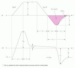
In Part 1, we discussed the body diode, which is a PN junction diode that lies inside of the MOSFET, between the n- region in the drain and the P-well in the source. Not unlike any other PN junction (Fig. 1), the carriers must recombine for the device to turn off, which takes time.
It’s important to understand how this diode works in applications such as synchronous buck converters and half- and full-bridge converters. When perusing a MOSFET datasheet, key body-diode characteristics to consider are the device’s trr and Qrr and the test conditions under which they were measured.
Shortly after the body diode is forward-biased, the MOSFET switches on. At this time, the body diode must be turned off and the current must flow through the channel of the device. The MOSFET’s reverse-recovery current then flows through the channel of the device along with the freewheel current from the inductor. This added current can negatively impact the safe operating area or SOA of the device.
Of the applications I’ve handled, the one with the most issues is in the low-side switch of the synchronous buck converter, also called the freewheel switch or sync FET. Under heavy load, when the high-side switch turns off, the inductor freewheels through the body diode of the low-side MOSFET. This is a lossy mode, which most controllers attempt to minimize by quickly enhancing or turning on the low-side switch. However, the event still occurs for a short time.
At this point, the only option seems to be choosing a device with lower Qrr and/or trr. Not true. We can put a device with a lower VF in parallel with the body diode so the freewheel current flows through the lower VF and not the body diode.
MOSFETs with built-in Schottky diodes, called FETkeys, offer an intrinsic Schottky diode in parallel with the body diode of the MOSFET that accomplishes the very same. The Schottky’s VF is far less than that of the PN junction. Thus, the Schottky conducts the freewheel current around the body diode. This exchanges the body-diode reverse-recovery event for a faster event in the Schottky with far less Qrr. (Remember that a Schottky is a majority carrier device… there’s nothing to recombine!)
In higher-voltage applications where FETkeys aren’t forthcoming, we can place a discrete Schottky of equivalent or higher voltage rating in parallel with the body diode with minimal inductance. If this alleviates the problem, you likely have a body-diode Qrr problem.
Avalanche and Flyback-Type Converters
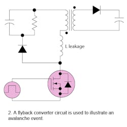
The easiest way to explain “avalanche” is to use a simple flyback-type converter (Fig. 2). For the sake of discussion, let’s assume that the RCD clamp structure used to minimize the voltage spikes across the switching MOSFET isn’t in-circuit. Also, the node between the MOSFET’s drain and the primary inductor (the switch node) is unclamped.
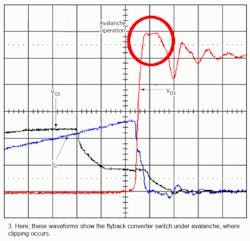
As further evidence, the slope of the flat top of the waveform will increase slightly over the clipped interval and possibly from one interval to the next (if there’s repetitive switching). This increasing slope corresponds to the positive coefficient of the internal body diode’s breakdown voltage.
Avalanche can also occur with parasitic inductances. For example, a large solenoid or motor will experience a similar voltage spike when opening the switch with an unclamped load.
This is all pretty straightforward and there are some magnificent articles and app notes that discuss avalanche ratings and design procedures in great detail. So, instead of repeating that information, I’d like to make a few suggestions on comparing MOSFET avalanche ratings from datasheet values.
In the bad old days, loads switched in an unclamped fashion were likely large inductive loads—perhaps a 300-mH lumped inductance series motor on a moon roof in a ’78 Lincoln Town Car, or a 500-mH solenoid on an older electric door lock plunger. As a result, the inductance values used to test and specify those parts were larger. These are, in fact, specified in the datasheet in the notes that appear around the avalanche ratings.
Fast-forward to the present. We now see loads for fuel injectors and transmission solenoids of just a few microhenries. As a result, newer MOSFETs use much smaller test inductors for avalanche testing. The new devices also note these values in the datasheets. What’s important here is to understand the difference when comparing MOSFETs side by side for avalanche ratings.
Older devices with larger inductors had relatively slow avalanche events. The inductance was large, so it took longer to ramp to the test current and LI2/2 energy level. These types of avalanche ratings usually pushed the thermal limits of the part and little else. The current didn’t ramp high enough to stress bondwires, etc.
New MOSFETs use a much smaller test inductance. The current ramps up much more quickly to the test value, and the test current is much higher. Avalanche ratings of these parts are usually determined by the I2t value of the bondwires, which is a faster mechanism than the thermal limit of the part. When compared side by side, the newer FETs will look like they have a severely reduced avalanche rating when compared to the older devices. We need to carefully consider the conditions of the avalanche test before reaching conclusions on which part may be better for a given application.
What is Linear Mode?
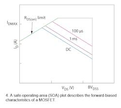
When it comes to linear mode, most datasheets don’t depict what’s truly going on in their SOA curves. An SOA curve is a log/log plot with VDS on the horizontal axis and ID on the vertical axis. This curve describes the forward-biased characteristics of the MOSFET. A positive slope of 1 decade(I)/decade(V) corresponds to a constant resistance, and a negative slope of 1 decade per decade corresponds to a constant power.
When the switch is turned on, we begin ramping up a current in the primary inductor as per V = –Ldi/dt. When the switch turns off, the polarity of the voltage drop across the inductor changes instantaneously, adding to the B+ voltage when viewed from the switch node. The inductor will “fly back” to a voltage high enough to maintain current flow and discharge the primary inductance.
With an unclamped switch node, and a MOSFET VDS voltage close to or slightly above the B+ voltage, we will see avalanche (Fig. 3). The avalanche signature is when the voltage across the MOSFET rises up quickly and then clips at some potential above the VDS rating of the device (usually 110% to 115% of VDS rating). Clipping occurs when the breakdown voltage of the MOSFET’s internal body diode limits the voltage excursion.
At very low voltages, the device simply can’t conduct the rated current due to the RDS(on) of the channel and the low VDS. This constant RDS(on) line forms the first part of the SOA curve (Fig. 4). The second part of the curve shows the device’s maximum current threshold. The third part of the curve, which depicts the constant power that the device can handle, has a –1 decade(I)/decade (V) slope. The fourth part of the curve is never discussed or depicted, other than in the newer IR datasheets. This segment has a negative slope of greater than the constant power. In fact, it almost looks like second breakdown in a bipolar junction transistor (BJT), only it is not. Rather, device stability is shown—the voltages are high and the currents are lower than the maximum rating.
Most switch-mode devices completely avoid this state via converter operation. In a switching power supply, the device is either in the on state, with low VDS and high currents (upper left on the SOA curve), or it is off. For the latter, it either blocks so the body diode is reverse-biased, the currents are low, and the voltages high (lower right on the SOA curve); or the body diode is conducting, creating a low negative VDS and high currents (not depicted on the forward-biased SOA curve at all).
The second break point of the SOA curve shows the Spirito boundary. In the mid 1990s, Italian researcher P. Spirito discovered that MOSFETs were failing at higher voltage and lower current datapoints, even though they fell well within the SOA curve. This inflection point is due to microscopic device properties. If a power MOSFET consists of many thousands of cells in parallel, we extensively employ metallization to ensure each cell has the same VDS and VGS voltages.
One parameter that does vary slightly from cell to cell is gain. If the gain of a cell is higher, this won’t be seen when we drive the device into saturation. However, it can be seen in linear mode. The cell with higher gain will have higher drain current, which will cause localized heating. As the device heats up and thresholds drop, thermal runaway may occur, which was the central theme of Spirito’s work.
Runaway isn’t an issue with saturated devices, since they share current very well between cells. Older, planar technology devices are safe, too. They feature lower cell densities and lower gains, thereby spreading the heat over larger areas and desensitizing the device to runaway condition in linear mode.
It’s a mouthful, but the point is simple: Older planar devices (Fig. 5) are better suited for linear operation than trench devices. This is best illustrated a side-by-side comparison of three different process technologies—an older planar process, a newer planar process, and a trench process. For a device in linear mode with constant VGS, ID, and temperature, increased temperature (with VGS held constant) and rising current results in thermal runaway and instability. Conversely, lessening current with increasing temperature results in a stable device that’s well suited for linear operation.
Looking at the curves, we see a clear crossover point for the early planar device, after which heating causes the same or less current for a given VGS. This doesn’t occur with the newer planar device and the trench device. The newer planar and trench devices aren’t suitable for hot-swap or linear regulation, since they will run away in linear mode.
Hot-swap, active ORing, and linear applications require planar FETs. But the datasheets don’t tell us which devices were made in which process. This is point where you grab hold of your local field application engineer, who can provide that information. I’ve seen hundreds of applications where a trench device is applied as a low-dropout (LDO) or hotswap controller, only to have catastrophic failures well within the purported SOA of the device. We can help you find the right part for the job!
From capacitive turn-on mechanisms to linear modes of operation, we’ve certainly covered a lot of material. This overview should assist most bench troubleshooting and prototype work. While I didn’t quantify a lot of parameters and guidelines, I did make an honest attempt to explain the main mechanisms, interactions, and possible fixes. Until I compiled this, I hadn’t run across anything collective on all of the different “quirks” of MOSFETs, although I’ve seen articles on most of the topics, especially avalanche and Cdv/dt turn-on mechanisms. Whether designing a dc-dc converter or a hotswap circuit, this material is applicable on all levels from milliwatts to megavolt-amps.
Original publish date: April 22, 2010
Updated July 22, 2024
About the Author
Paul Schimel
Senior Field Applications Engineer
Paul Schimel is a senior field applications engineer at International Rectifier. He has more than 15 years experience in power electronics design, EMC, and transformer design including offline ac-dc converters for medium and high power levels, motor drives, and dc-dc converters. He is a hands-on engineer and innovator, endlessly building power electronics circuitry, welding, and machining for audio, HVAC, and propulsion applications. Also, he is a licensed Professional Engineer and holds two patents. He can be reached at [email protected].
Voice Your Opinion!
To join the conversation, and become an exclusive member of Electronic Design, create an account today!

Leaders relevant to this article:


