Virtually all switching power supply designs include a closed control loop with negative feedback from the output to input. This requires a compensation network to adjust the supply’s closed loop frequency response to ensure stability and optimize transient response. Today, some voltage regulator ICs employ automatic compensation that simplifies and improves this design task. For more information, see the sidebar “Voltage Regulator Compensation”.
To understand the auto compensation technique, we first have to retrace evolution of this technology. One of the earliest compensation techniques provided a voltage regulator with external nodes so the designer could insert compensation components. Determining compensation component values involved an analysis of the poles and zeroes associated with the regulator IC and its external components. After determining the required compensation, the designer modeled or measured the regulator circuit with the compensation components installed. This process usually required several iterations before obtaining the desired results.
Proper implementation of a compensation network required engineers with special tools, skills and experience. If the circuit was modeled and not measured, the designer had to eventually insert the actual compensation components to measure supply performance. Modeling was only as good as the designer’s knowledge of the components and parasitics. The model might have been incomplete or differed from the actual circuit, so compensation had to be verified by measurement of the actual circuit. Invariably, reworking was necessary because of possible errors associated with changing components. Reworking could also change supply performance and damage circuits powered by the regulator.
Some regulator IC vendors included internal compensation components, so the design didn’t need further analysis. However, the designer had to use external vendor-specified components.
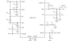
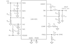
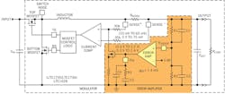
A single compensation node was the next stage in this evolution. An example of this is Texas Instruments’ LM21305 switch-mode regulator IC (Fig. 1). The LM21305 typically requires only a single resistor and capacitor for compensation. However, sometimes it required another capacitor.
Fig. 1.The LM21305 is a switch-mode regulator IC that employs a single compensation node the requires compensation components Rc and Cc1 connected between the COMP pin and AGND.
Even though you could determine and insert compensation components their values could vary with temperature and from unit-to-unit in production; this could affect voltage regulator performance. Plus, component values could change over time and impact performance. Thus, you couldn’t ensure optimum long-term performance based on the values and quality of compensation components.
Auto Compensation
To eliminate the problems associated with manual power supply compensation several companies developed the technology for automatic compensation. This resulted in mixed-signal regulator IC designs employing automatic compensation. This relieved the designer of the need for special tools, knowledge or experience to optimize performance. Automatic compensation sets the output characteristics so that changes due to component tolerances, ageing, temperature, input voltage and other factors do not affect performance.
CUI (Tualatin, OR) has three families of digital point of load modules that incorporate auto compensation: NDM2Z, NDM2P, and NSM2P. The NDM2Z uses the Intersil/Zilker ZL8101M regulator IC, whereas the NDM2P and NSM2P use the Powervation PV3012
regulator IC. Auto compensation bypasses the traditional practice of building-in margins to account for component variations, which can lead to higher component costs and longer design cycles.
Although functionally similar, the NDM2P employs I2C connectivity and the NSM2P does not. This allows the NDM2P to be controlled by a host processor that can exercise PMBus commands.
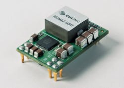
Fig. 2. CUI’s NDM2Z power supply employs auto compensation that allows it to dynamically set optimum stability and transient response.
The 50 A NDM2Z (Fig. 2), NDM2P, and NSM2P deliver 91% efficiency with 12 Vdc input and a 1.0 Vdc output at 50% load. These point-of-load modules all have a 4.5 to 14 Vdc input range and a programmable output of 0.6 to 5.0 Vdc in the 12 A version and 0.6 to 3.3 Vdc in the 25 A and 50 A versions. Table 1lists the modules’ size.
Module features include active current sharing, voltage sequencing, voltage tracking, synchronization and phase spreading, programmable soft start and stop, as well as a host of monitoring capabilities. CUI’s simple, easy to use Novum ACE™ GUI aids these designs.
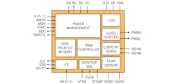
The NMD2Z uses an Intersil/Zilker ZL8101, voltage-mode, synchronous buck controller with a constant frequency pulse width modulator (PWM). This third generation digital controller uses a dedicated, optimized, state machine for generating precise PWM pulses and a proprietary microcontroller used for setup, housekeeping, and optimization. It requires external drivers, power MOSFETs, capacitors, and inductors (Fig. 3). Integrated sub-regulation allows operation from a single 4.5V to 14V supply. Using simple pin connections or standard PMBus commands you can configure an extensive set of power management functions with Intersil’s PowerNavigator GUI.
Fig. 3. Intersil/Zilog’s ZL8101 IC block diagram shows the PWM outputs (PWMH and PWML) that interface with an external driver like the ZL1505.
Initially, the ZL8101’s auto compensation measures the characteristics of the power train and determines the required compensation. The IC saves compensation values and uses them on subsequent inputs. Once enabled, the ZL8101 is ready to regulate power and perform power management tasks with no programming required. Advanced configuration options and real-time configuration changes are available via the I2C/SMBus interface. An on-chip non-volatile memory (NVM) saves configuration data.
The ZL8101’S digital PWM loop interfaces with external drivers, such as the Intersil/Zilker ZL1505. It can work with other drivers having 2.5 V to 5.5 V inputs, including DrMOS devices and Intersil’s ISL6611 phase doubler driver.
You should choose the external power MOSFETs primarily on RDS(ON) and secondarily on total gate charge. The actual power converter’s output current depends on the characteristics of the drivers and output MOSFETs.
Configurable circuit protection features continuously safeguard the IC and load from damage due to system faults. The ZL8101 continuously monitors input voltage, output voltage/current, internal temperature, and temperature of an external thermal diode. You can also set monitoring parameters for specific fault condition alerts.
A non-linear response (NLR) loop improves the response time and reduces load transient output deviations. To optimize power converter efficiency, the ZL8101monitors its operating conditions and continuously adjusts the turn-on and turn-off timing of the high-side and low-side power MOSFETs. Adaptive performance optimization algorithms such as dead-time control, diode emulation, and adaptive frequency provide greater efficiency improvement.
A Power-Good (PG) signal indicates the output voltage is within a specified tolerance of its target level and no fault condition exists. By default, the PG pin asserts if the output is within -10%/+15% of the target voltage. You can change these limits and the polarity via the I2C/SMBus interface.
An internal phase-locked loop (PLL) serves as a clock for internal circuitry. You can drive the PLL from an external clock source connected to the SYNC pin. You can set the switching frequency from 200 kHz to 1.33 MHz.
A Windows™-based GUI enables full configuration and monitoring capability via the I2C/SMBus interface.More Auto Compensation
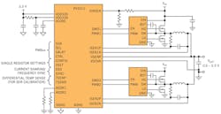
Fig. 4.Powervation’s PV3012 IC is a real-time auto compensation IC with a single output, dual or single phase digital synchronous buck controller for POL applications.
Powervation’s PV3012 used in CUI’s NDM2P and NSM2P modules is a single output, dual or single phase digital synchronous buck controller with real-time adaptive loop compensation, for point-of-load (POL) applications (Fig. 4). Operating from a 3.3 V supply it can provide a programmable 0.6 V to 5.5 V output. You can configure and control it with the PMBus, a single resistor, or through programming stored in NVM. Its auto compensation provides operational flexibility for loads that can change over a supply’s lifetime.
To implement closed loop compensation, the PV3012 uses a discrete-time adaptive control algorithm updated in real-time, on a switching cycle-by-cycle basis. This self-compensating adaptive control for DC/DC power conversion employs the PV3012’s proprietary Auto-Control® technology. Should the power supply conditions or environment change over time, Auto-Control constantly monitors control system performance and adjusts the controller‘s compensation coefficients.
Auto-Control eliminates external compensation components and the need to manually retune compensation if load characteristics change. Optimized for high perfor mance with low power consumption, its DSP core’s adaptive algorithm is independent of general housekeeping, fault management and configuration tasks.
A low-latency precision analog-digital converter (ADC) samples and quantizes voltages, currents, and temperatures. The DSP accepts these results, solves the resulting matrix and adjusts the digital pulse-width modulator (DPWM) output on a cycle-by-cycle basis. The DPWM provides duty cycle resolution of at least 15 Bits, effectively eliminating limit-cycling and quantization noise. The power management processor also receives the ADC results, providing these values through the PMBus communication interface for remote measurement and reporting of current, voltage, and temperature information. To maximize system performance and reliability, the IC also provides temperature correction/compensation of several parameters.
When used in dual phase mode, phases may be shedded as the load varies, which maximizes efficiency over the load range. Additionally, interleaved outputs of each phase doubles the effective switching frequency. With Powervation’s Digital Stress Share™ (DSS) and PLL synchronization, you can parallel multiple PV3012s to increase the number of phases supporting the application’s load.
The PV3012 utilizes analog and digital functionality to maximize system protection by continuously monitoring the health of the power conversion system. It generates fault and warning conditions, protects the power stage, and actively manages system re-start attempts. It monitors under- and over-voltage (UVLO, OVLO) conditions on the input and output. It monitors and implements two over-current monitors: one fast analog (SCP) for protecting external circuits and the other(OCP) calculated from ADC readings for system use. Temperature monitoring is available from an on-chip sensor or external sensor.
Using the PowerSMART™ GUI design tool the designer can communicate with the PV3012 controller to receive/monitor information from the power supply and IC, as well as program settings to the controller. This allows the designer to view the power supply’s status, input/output voltages, output current, phase current sharing, and fault conditions detected by the controller.
Architecture for digital power management solutions is a multi-processor system-on-chip (SoC) with an ultra-lean proprietary dual core DSP and RISC processors. It contains both RAM and NVM, power conversion blocks, SMBus serial interface, ADCs and DACs (digital-to-analog converter), and oscillator and phase lock loop timing sources.
The DSP provides computational capability for complex algorithms, such as the Auto-Control® real-time loop compensation. The 16-bit, 64 MHz RISC provides fast instruction execution and eliminates overhead and power dissipation for other processing options.
NVM stores both program and PMBus codes. When powered on, the contents of the NVM load into RAM for fast access to the processing unit. The NVM serves as a long-term storage of code that determines power supply function data stored over elevated temperatures and time.
Sidebar: Voltage Regulator Compensation
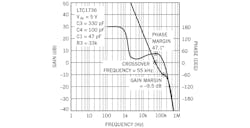
Fig. 5. Bode plot for the LTC1736 regulator IC shows crossover frequency, gain and phase margin for the circuit in Fig. 6.
Fig. 6. LTC1736 regulator IC circuit showing it compensation components connected to the ITH pin.
Gain and phase of the closed loop voltage regulator varies with frequency, as shown in Fig. 5, a Bode plot for the LTC1736 circuit in Fig. 6. Key to a voltage regulator’s Bode plot are the poles and zeroes of each component. Each pole has a corner frequency, caused by a resistance and capacitance that determine the beginning of a 20dB/decade drop in voltage gain. The pole also causes the phase to decrease by 90°. A zero has the opposite effect, it causes the gain to increase by 20dB/decade starting at its “RC” corner frequency and adds 90° of phase shift, The effects of poles and zeros are additive, so that two poles at the same frequency cause a 40dB/decade roll-off in gain and a 180° phase shift over two decades. If a pole and zero occur at the same frequency, their effects cancel. The frequency at which the control loop gain crosses through unity (0 dB) is the crossover frequency that determines the regulator’s bandwidth and transient response.
Using a network analyzer you can determine stability margins by measuring the gain and phase of the control loop, and then observe the resulting Bode plot. Phase margin is the difference between the signal phase and – 360° when the voltage gain is unity (0dB). A 60° phase margin is preferred, but 45° is usually acceptable. The gain margin is the amount of negative gain present when the signal phase is zero (–360°). A gain margin of –10dB is usually considered acceptable. Gain and phase margin are important because actual component values may vary over temperature. Thus, component values may differ from unit-to-unit in production, causing the control loop’s voltage gain and phase to vary accordingly. Plus, component values may vary over time, and cause instability.
If component values cause the phase to go to zero at the crossover frequency, the regulator becomes unstable and oscillates. The goal of compensation is to provide the best gain and phase margins with the highest possible crossover frequency. A high crossover frequency provides a quick response to load current changes, whereas high gain at low frequencies produces fast settling of the output voltage. Component values and transfer function variations can force a trade-off between high crossover frequency and high stability margins.
