Buck-Boost µModule Devices Regulate VOUT, Even When VIN is Above or Below VOUT
A family of buck-boost µModule® (micromodule) regulators from Linear Technology, the LTM8055 andLTM8056, seamlessly regulate VOUT regardless of whether VIN is equal to, greater or less than VOUT. Housed in a 15 mm x 15 mm x 4.92 mm BGA package, these devices include a current mode controller, power switching elements, power inductor and a modest amount of input and output capacitance.
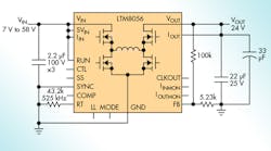
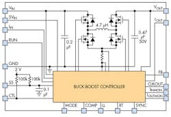
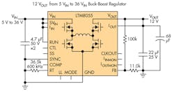
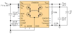
The LTM8055 and LTM8056 are standalone non-isolated buck-boost switching DC/DC power supplies. Fig. 1 is a simplified block diagram of the LTM8055, which is similar to the LTM8056 except for the value of its output capacitor. Their buck-boost topology allows them to regulate their output voltage. An example is shown in Fig. 2 where an LTM8055 produces a regulated 12V out even though the input varies from 5 V to 36 V. Fig. 3 is an LTM8056 circuit that provides 24 V with a 7 V to 58 V input. For the lower voltage it is a boost converter and for the higher voltage it is a buck converter.
With one resistor, you can set output voltages for either device. An LTM8055 operates with input voltages ranging from 5 V to 36 V, and can drive a load up to 8 A. The LTM8056 handles input voltages up to 60 V, with 4 A load capability. They may be operated at lower input voltages if SVIN is powered by a voltage source above 5 V.
You set the output voltage for both µMicromodules by connecting the FB pin to a resistor divider between VOUT and GND. Besides regulating their output voltage, both are equipped with average current control loops for the input and output. Adding a current sense resistor between IIN and VINlimits the input current below some maximum value. The IINMON pin reflects the current flowing though the sense resistor between IIN and VIN.
A current sense resistor between VOUT and IOUT allows the µMicromodules to accurately regulate their output current to a maximum value set by the sense resistor. When the resistor is present, the IOUTMON pin reflects the output current flowing through VOUT. Both devices should be used with an output sense resistor to limit the maximum output current, as buck-boost regulators can deliver large currents when the output voltage is lower than the input.
Although both µMicromodules do not require an output sense resistor to operate, they use information from the sense resistor to optimize their performance. If an output sense resistor is not used, their efficiency or output ripple may degrade, especially if the current through the integrated inductor is discontinuous. In some cases, an output sense resistor is required to adequately protect them against output overload or short-circuit.
A voltage less than 1.2 V applied to the CTL pin reduces the maximum output current. Drive CTL to about 50 mV to stop switching. If you require more output current than a single LTM8055 or LTM8056 can provide, you can operate multiple devices in parallel.
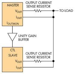
You can parallel two devices as a master and a slave, as shown in Fig. 4. Each device is equipped with an IOUTMONand a CTL pin. The IOUTMON pin’s 0 V to 1.2 V signal reflects the current passing through the output sense resistor, while a voltage less than 1.2 V applied to the CTL pin will limit the current passing through the output sense resistor. By applying the voltage of the master’s IOUTMON pin to the slave’s CTL pin, the two units will source the same current to the load, assuming each device output current sense resistor is the same value.
An internal regulator provides power to the control circuitry and the gate driver for the power MOSFETs. This regulator draws power from the SVIN pin. The RUN pin is used to shut down the LTM8055 and LTM8056, disconnecting the output and reducing the input current to less than 1 μA.
Both devices are equipped with a thermal shutdown that inhibits power switching at high junction temperatures. The activation threshold of this function is above 125°C to avoid interfering with normal operation. Prolonged or repetitive operation near the thermal shutdown temperature may damage or impair device reliability.
PWM Control
LTM8055 and LTM8056 are fixed frequency PWM regulators. For both, connecting an appropriate resistor from the RT pin to GND adjusts the switching frequency from 100kHz to 800kHz, whereas each device can be synchronized to an external clock frequency from 200kHz to 700kHz. Driving the SYNC pin will synchronize them to an external clock source. The CLKOUT pin sources a signal that is the same frequency but approximately 180° out of phase with the internal oscillator.
The CIN and COUT capacitor values in Figs. 2 and 3 should be low ESR ceramic types. However, not all ceramic capacitors are suitable. X5R and X7R types are stable over temperature and applied voltage and give dependable service. Other types, including Y5V and Z5U have large temperature and voltage coefficients of capacitance, so if they are used they may have only a small fraction of their nominal capacitance, resulting in higher than expected output voltage.
Another precaution regarding ceramic capacitors concerns the maximum input voltage rating of the µMicromodules. A ceramic input capacitor combined with trace or cable inductance forms a high Q (underdamped) tank circuit. If the circuit is plugged into a live supply, the input voltage can ring to twice its nominal value, possibly exceeding the device’s input rating.
Soft-Start
Soft-start reduces the input power sources’ surge currents by gradually increasing the controller’s current. As illustrated in Fig. 2, the LTM8055 and LTM8056 have an internal soft-start RC network. Depending upon the load and operating conditions, the internal network may be sufficient for the application. To increase the soft-start time, simply add a capacitor from SS to GND.
Both devices employ an accurate average output current limit set by an external sense resistor placed between VOUTand IOUT as shown in Figs. 2 and 3. VOUT and IOUTinternally connect to a differential amplifier that limits the current when the voltage VOUT-IOUT reaches 58mV. The current limit, IOUT(LIM), is:
Where:
RSENSE = Value of the sense resistor in ohms
The LTM8055 and LTM8056 are switching power supplies, so take care to minimize EMI and ensure proper operation. Even with the high level of integration employed in these devices, you can encounter problems.
A few rules to keep in mind:
1. Place the RFB and RT resistors as close as possible to their respective pins.
2. Place the CIN capacitor as close as possible to the VIN and GND connection of the LTM8055/6.
3. Place the COUT capacitor as close as possible to the VOUTand GND connection of the LTM8055/6.
4. Minimize the trace resistance between the optional output current sense resistor, ROUT, and VOUT. Minimize the loop area of the IOUT trace and the trace from VOUT to ROUT.
5. Minimize the trace resistance between the optional inputcurrent sense resistor, RIN and VIN. Minimize the loop area of the IIN trace and the trace from VIN to RIN.
6. Place the CIN and COUT capacitors such that their ground current flow directly adjacent or underneath the LTM8055/6.
7. Connect all of the GND connections to as large a copperpour or plane area as possible on the top layer. Avoid breaking the ground connection between the external components and the LTM8055/6.
8. Use vias to connect the GND copper area to the board’sinternal ground planes. Liberally distribute these GND vias to provide both a good ground connection and thermal path to the internal planes of the printed circuit board. Pay attention to the location and density of the
thermal vias. The LTM8055/6 can benefit from the heat sinking afforded by vias that connect to internal GND planes at these locations, due to their proximity to internal power handling components.
