Bidirectional, 2A Buck-Boost DC-DC Regulator Provides Fast Charging and System Backup Using Supercapacitors or Batteries
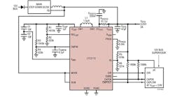
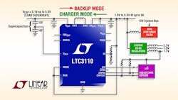
The LTC3110 from Linear Technology is a 2A buck-boost dc-dc regulator/charger combination with pin-selectable operation modes for charging and system backup (Fig. 1). This bidirectional, programmable input current buck-boost supercapacitor charger provides active charge balancing for 1- or 2-series supercapacitors. Its proprietary low-noise buck-boost topology does the work of two separate switching regulators, saving size, cost, and complexity.
Bidirectional operation refers to the dc current flow related to VSYS, the power supply pin for system backup output voltage and charge current input voltage (Fig. 1). In one direction the LTC3110 operates as buck-boost regulator, taking current out from the supercapacitor and providing a regulated voltage to the load at the VSYS pin. In the other direction the sign of the current flow reverses and an accurately limited current flows from the system rail back to charge the supercapacitor. If VSYS drops due to a power loss, it can switch direction autonomously to stabilize the system voltage by delivering current from the supercapacitor into VSYS.
The LTC3110’s 0.1V to 5.5V capacitor/battery voltage and 1.8V to 5.25V system backup voltage ranges make it well-suited for a variety of backup applications using supercapacitors or batteries, for example:
- It integrates all the functionality required to exploit the benefits of supercapacitors, charging, balancing. and backup.
- Its Input current limit eliminates external components, lowers IQ, and allows it to utilize full capability of a power source without exceeding safety limits.
- Input power sharing enables LTC3110 and other dc/dc converters or loads to share the same power source with minimal derating/margin.
- An active balancer synchronously shuttles charge between multiple capacitors, eliminating external ballast resistors and their resultant power losses, resulting in fewer recharge cycles and faster charging.
- It can autonomously transition from charge to backup mode or switch modes based on an external command.
Charge or Backup
The DIR pin (Fig.1) is the charge/backup mode selector input with hysteresis. The DIR pin’s rising threshold is 1.095V and its falling threshold is 1.045V. A voltage on the DIR pin above the rising threshold enables the charger mode. A voltage below the falling threshold enables the backup mode. The pin can be driven digitally, e.g., from a μC. With the help of an external resistor divider the pin can be configured as voltage supervisor input monitoring any system voltage.
VCAP (Fig. 1) is a bidirectional power pin for connection to supercap backup capacitor(s) or backup battery(ies). In the charge mode a current flows out of pin VCAP to charge the storage elements connected between VCAP and PGND. When in backup mode, the current flows into the VCAP pin and the stored energy is used to backup the load on VSYS.
In the charge mode the main power system is active, so the LTC3110 can autonomously or through user command reverse the direction of power flow using the regulated system voltage to charge and balance the supercapacitors. VCAP is efficiently charged to above or below VSYS by the buck-boost PWM.
While charging, the integrated linear charge-balancing buffer regulates the mid-voltage, VMID (Fig. 1), of a stack of capacitors to half of VCAP, thus equalizing out voltage mismatches of top and bottom capacitor. If the capacitor mismatch exceeds the current capabilities of the charge balancer, charging is suspended until VMID comes back to half of VCAP. The suspend charge function is only active for VCAP > 2.2V = VTH(CHRG) (voltage charge threshold) with hysteresis. For VCAP < 2V, charger operation is always continuous.
Charge Balancing
The LTC3110’s active charge balancing eliminates the constant drain of dissipative external ballast resistors, ensuring charging even with mismatched capacitors, and less frequent recharge cycles. Programmable maximum capacitor voltage regulation actively balances and limits the voltage across each capacitor in the series stack to one-half of the programmed value, ensuring reliable operation as capacitors age and develop mismatched capacities. The low RDS(ON), low gate charge synchronous switches provide high efficiency conversion to minimize the charging time of storage elements. The IC is ideal for safely charging and protecting large capacitors in backup power applications such as servers and RAID systems, and RF systems with battery/capacitor backup.
If the die temperature exceeds approximately 165°C, the IC will enter overtemperature shutdown, all switching will be inhibited, and the charge balancer disabled. Open-drain output pins CAPOK, CMPOUT, and CHRG may still pull down while in thermal shutdown. The IC will remain disabled until the die cools by approximately 10°C. The soft-start circuit is reinitialized in overtemperature shutdown to provide a smooth recovery when the fault condition is removed.
You can program the charge-mode average input current limit up to 2A with ±2% accuracy, using a resistor from the PROG pin ground. This prevents system power source overload while minimizing capacitor recharge time. Average input current is accurately controlled over a 0.125A to 2A programming range. Pin-selectable Burst Mode operation improves light-load efficiency and reduces standby current to only 40µA, and shutdown current to less than 1µA.
In backup mode, the IC maintains a system voltage, VSYS, of 1.71V to 5.25V, powered from the supercapacitor stored energy. The VCAP pin is the bidirectional power pin for connection to supercapacitor backup capacitor(s) or backup battery(ies). VCAP features a practical operating range from 5.5V down to 0.1V. This ensures that all practical stored supercapacitor energy is utilized, thereby extending backup times or shrinking the storage capacitors.
Other features of the LTC3110 include 1.2MHz switching frequency to minimize external component size, thermal overload protection, two voltage supervisors for direction control and end of charge, and one general purpose comparator with an open-collector output for interfacing with a microcontroller or microprocessor.
The power switches in the LTC3110 are designed to operate continuously with currents up to the internal current limit thresholds. However, when operating at high current levels there may be significant heat generated within the IC. As a result, careful consideration must be given to the thermal environment of the IC in order to optimize efficiency and ensure that the LTC3110 is able to provide its full-rated output current. Specifically, the exposed pad of both the QFN and TSSOP packages should be soldered to the PC board and the PC board should be designed to maximize the conduction of heat out of the IC package.
VSYS Voltage Programming
You can set the VSYS voltage with an external resistor divider connected to the FB pin as shown in Fig.1. The resistor divider values determine the VSYS backup voltage according to:
VSYS = System backup output voltage and charge current input voltage
RTOP = Top resistor in ohms (1910k in Fig. 1)
RBOT = Bottom resistor in ohms (523k in Fig. 1)
The buck-boost converter utilizes voltage mode control and in addition to setting the VSYS voltage, the value of RTOP plays an integral role in the dynamics of the feedback loop. In general, a larger value for RTOP will increase stability and reduce the speed of the transient response. A smaller value of RTOP will reduce stability but increase the speed of the transient response. A good starting point is to choose RTOP = 1MW and then calculate the required value of RBOT to set the desired VSYS voltage according to Equation (1). If a large VSYS capacitor is used, the bandwidth of the converter is reduced. In such cases, RTOP can be reduced to improve the transient response. If a large inductor or small VSYS capacitor is utilized, the loop will be less stable and the phase margin can be improved by increasing the value of RTOP.
The choice of inductor used in LTC3110 application circuits influences the maximum deliverable backup and charge current, the magnitude of the inductor current ripple, and the power conversion efficiency. The inductor must have low dc series resistance or current capability and efficiency or it will be compromised. Larger inductance values reduce inductor current ripple and generally yield greater backup current capability. For a fixed dc resistance, a larger value of inductance will yield higher efficiency by reducing the peak current to be closer to the average backup current and therefore minimize resistive losses due to high RMS currents. However, a larger inductor within any given inductor family generally has a greater series resistance, thereby counteracting this efficiency advantage. An inductor used in these applications should have a saturation current rating that is greater than the worst-case average inductor current plus half the ripple current.
Housed in a compact, thermally enhanced 24-lead and TSSOP 4mm x 4mm QFN package, the LTC3110 has E- and I-grade operation from -40°C to 125°C, and up to 150°C for the high-reliability H grade.


