This file type includes high resolution graphics and schematics when applicable.

Analog-to-digital converters (ADCs) and digital-to-analog converters (DACs) have been around since the beginning of the digital age. With the introduction of the single-chip DSP pioneered by Texas Instruments in the late 1970s and early 1980s, engineers had the tools for building systems that could easily surpass the performance of their analog counterparts.
Early data converters were relatively slow and used parallel interfaces to connect to the DSP or processor. As process technology improved, so did the speed and dynamic range (number of bits) of the data converters. This led to data converters requiring faster and wider buses.
Today, modern data converters can easily exceed conversion rates of a gigasample per second at 12 or more bits of resolution, which represents a bus transfer rate of greater than 1.5 billion bytes per second. This presents a challenge for engineers when laying out printed-circuit boards to connect the convert to a DSP, processor, or FPGA. The problem gets harder when there are multiple ADCs or DACs that require their analog inputs or outputs to be phase-coherent. This requires that parallel buses have matched electrical lengths and deterministic latency—a layout nightmare.
Serialization
Early on, the industry recognized this problem even before the introduction of ultra-high-speed data converters, and introduced serialized low-voltage differential signaling (LVDS) interfaces to minimize the number of interconnections. This interface simply serialized the parallel bus and provided an LVDS bit clock to recover the data. Routing was still an issue due to the relationship of the clock and data paths.
It did, however, allow for multiple data converters in a package with a single clock, and in some applications is still used today to minimize pin count. An example is Texas Instruments’ ADC3445, which contains four 125-Msample/s, 14-bit ADCs in a single 48-pin, 8-mm-square package.
Early in the 21st century, it was apparent that as data-converter speeds increased, routing became an issue. It thus drove the formation of the JEDEC Solid State Technology Association standard “JESD204” in 2006. This standard continues the concept of a serialized interface using a 3.125-Gb/s link rate, and introduces coding and framing, which removes the need for a separate data clock. The original standard provided only a single lane and lacked a synchronization method, so a common “frame clock” was required when locking multiple data converters for phase coherency.
By April of 2008, JEDEC released the “A” revision, which introduced multiple aligned lanes for higher throughput, but still required a common frame clock for synchronization. It was followed in July of 2011 by the current “B” revision of the standard. This version increased the lane speed to 12.5 Gb/s, along with introducing support for deterministic latency (very important for phase coherency) as well as an intrinsic method for data-converter synchronization.
The Physical Interface
A JESD204B interface contains one or more high-speed, mono-directional, current-mode-logic (CML) differential pairs, which carry the data converter’s data. This is referred to as a “lane.” The number of lanes is not tied to the number of converters as in the serialized LVDS interface. But like PCI Express, it provides greater bandwidth in the interface. This is a common misconception when moving to JESD204B.
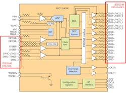
There are three other critical pins: the device clock (DEVCLK) formally known as “frame clock” in earlier revisions; the system reference signal (SYSREF); and an active low synchronization pin (/SYNC). Depending on the mode of the device (see the Interface Subclasses section), these additional pins are used in various ways to time both the analog conversions and the movement of data between the data converters and the processing element (Fig. 1).
DEVCLK is used by the data converter to derive several other internal clock signals: the data converters internal frame clock used to transport data; the sampling clock used to time the conversion; and the local multi-frame clock (LMFC) that’s used to establish deterministic latency (more on this later). SYSREF is a phase-reference signal that derives the LMFC in subclass 1 (not used in subclass 0 or 2). The /SYNC signal is used for data transport synchronization in all subclasses as well as the LMFC phase reference in subclass 2.
The Data Format
Unlike simple serialized LVDS interfaces, JESD204B uses a model similar to Internet Protocol or the Open Systems Interface (OSI) model that has layers in which each performs a function. The encoder side performs the functions of each layer one by one, and the receiver performs the inverse function in the opposite order to reconstruct the data.
Each layer is responsible for performing various functions in the reliable passing of data between the transmitter and the receiver. In the JESD204B standard there are four layers: transport, scrambling (optional, but desired), data link, and physical.
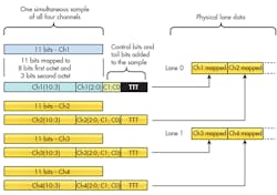
The transport layer is one of the more complex functions, which maps the data to octets (groups of 8 bits or a byte). The layer then maps to frames consisting of multiple octets on the transmit side, and in reverse order for the receive side. This is quite simple for an 8-bit data converter, but for anything else, such as an 11-bit data converter, it gets more complicated. It also inserts control bits into the stream that are used to communicate status information to the receiver (Fig. 2).
The optional scrambling layer is used to randomize data patterns to minimize noise and correlated signals in the system. It uses a fixed polynomial of 1 + X^14 + X^15, which is implemented with serial feedback shift registers and exclusive “OR” gates that are symmetrical in encoding and decoding. This simple method of spectral-spreading allows the receiver descrambler to lock after receiving only two octets from the link layer. Although this function is optional, it’s highly recommended for the best spectral purity.
The data link layer is responsible for the 8b/10b coding, which converts the octets to 10-bit standard symbols and back. This layer also manages establishing a working link, including frame and lane alignment. Several of the standard 8b/10b symbols are reserved for this function as well as monitoring the link health. The coding does come with a 20% overhead penalty. Future versions may move to a higher level coding, such as 64/66b, to regain lost bandwidth in the interface.
Finally, the physical layer is simply the drivers and receivers that electrically move the bits and the clock-data-recovery (CDR) circuitry. The physical interface utilizes ac-coupled CML drivers and receivers. The 8b/10b coding provides dc balancing and prevents baseline wander when ac-coupled. The coding also delivers enough edge transitions for the CDR to quickly lock on the data during link establishment.
To summarize, the four layers are used to establish a link between a data converter and a processing element, and reliably transport the data converter’s data and control information from the transmitter to the receiver.
Interface Subclasses
To provide a method for backward-compatibility, JEDEC introduced a concept of “subclasses” to tailor the interface for different modes of operation. Subclass 0 is the compatibility mode with the “A” revision, but also supports the higher lane rate of 12.5 Gb/s. As in the “A” revision, this mode supports multiple synchronized data converters, but has no support for deterministic latency.
Although the latency between data converters may be fixed, it varies at startup. This requires the system designer to provide a solution to determine when the data from each data converter arrives at the FPGA or processors. Also note that SYSREF is not used in this mode.
Subclass 1 provides deterministic latency and intrinsic multi-device synchronization. This is accomplished by using the internal frame and local multi-frame clocks along with the SYSREF clock signal. The internal frame clock is used for the serial transfer of symbols between the data converter and the processing element, while the LMFC provides a reference to a known latency.
DEVCLK, along with the phase of the SYSREF signal, determine the internal frame clock and LMFC. Because of the close relationship of DEVCLK and SYSREF in this mode, SYSREF must be source synchronous with the device clock. This will this constrain the layout to electrically match these two signals. However, the data lanes needn’t match, and it relieves the SYNC timing found in subclass 0.
In subclass 2, each device has the same internal frame clock and LMFC, as found in subclass 1. However, the SYNC signal is now used for synchronization and the deterministic latency. In this mode, the phase of the SYNC signal is used to align the internal frame clock and LMFC, and now must be source-synchronous with DEVCLK. Due to the tight timing requirements for DEVCLK and /SYNC, this mode is not recommended for extremely high sample rates.
Establishing a Connection
Now that the basics have been covered, it’s time to discuss how this all ties together to get an analog signal to or from the processing element. Before the data conversion can begin, several states must be established. This is where many engineers struggle due to the many configuration options of this interface along with the complexity of instantiating a JESD204B interface when using an FPGA.
To begin, a link between the data converter and the processing element needs to be established. This is accomplished by asserting the active low signal /SYNC (input to the transmitter side). The transmitter interface then begins sending K28.5 comma symbols to allow both the receiver CDR to phase-lock to the bit stream and find the character boundary of the data stream. Note that if the link has multiple lanes and operates in subclass 0, then the /SYNC signals must be combined and presented to the transmitter simultaneously. Subclasses 1 and 2 don’t have this requirement.
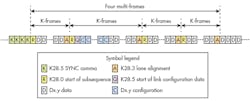
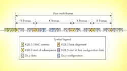
After achieving code group synchronization (CGS), /SYNC is de-asserted. Then on the next non-K28.5 symbol, the receiver will align its frame boundary. This begins the initial lane synchronization (ILA) sequence, which is used to align multiple lanes. Note that this sequence is never scrambled, even if scrambling is enabled. The ILA, which transfers data on the configuration of the transmitter side, is four multi-frames long. A multi-frame begins with a K28.0 symbol (start of subsequence) and ends with a K28.3 symbol (lane alignment character) (Fig. 3).
Once the four multi-frames are transmitted, scrambling is turned on (if enabled) and user data is transferred to the receiver. A helpful tip is to utilize the diagnostic capability built into many data converters or FPGA JESD204B IP blocks. Many contain an option that feeds a known pattern, such as a ramp or sine wave, to the transport layer. These patterns often use the full dynamic range of the data converter to simulate real converted data.
Optionally, at the transport layer, a pre-determined octet pattern can be inserted in place of the data converter test pattern, which is simpler than test patterns for debugging. During bring-up, turn scrambling off to make patterns easier to spot when using a logic analyzer or FPGA code to monitor lane traffic.
Conclusion
The JESD204B standard is far more complex than what was covered in this article. However, for those not familiar with its operation, this overview may provide some insight for implementing the interface. As data-converter speeds increase, this standard will undoubtedly continue forward and expand to provide even higher throughput as well as additional complexity and control of the data converters that use this interface.
Reference:
TI JESD204B solutions
About the Author
Richard F. Zarr
Richard Zarr is a technologist at Texas Instruments focused on high-speed signal and data path technology. He has more than 30 years of practical engineering experience and has published numerous papers and articles worldwide. He is a member of the IEEE and holds a BSEE from the University of South Florida as well as several patents in LED lighting and cryptography.
Comment About the Article
To join the conversation, and become an exclusive member of Electronic Design, create an account today!

Leaders relevant to this article: