Define Analog Sensor Interfaces In IoT SoCs
Also known as “smart everything,” the Internet of Things (IoT) is grabbing headlines across the industry. As any great new technology, it comes wrapped in shiny paper that touts it as the solution for all things connected, be it the online tracking of the merchandise in a truck across the continent, the automatic sensing of the color of toast in the toaster, or measuring the number of steps walked in a day.
Looking beyond the hype and avoiding the scary potential of hackers taking over the fridge, this technology makes perfect sense for many uses.1 At the 2014 International CES, major industry players showed off their most recent toys (in some cases, literally) that benefit from this technology: wristbands and other wearables for medical, sports, and wellbeing applications; home appliances ranging from light control to the fridge; and even connected cars. While this market is still young, there is clear momentum driven by growing consumer adoption.
Emerging Applications
Although the IoT concept is loosely defined, it generally refers to applications working on the principle of distributed and remote collection of environmental data followed by limited local processing, then making the result available to the “world” via some sort of shared access to the Internet for further processing and aggregation. Applications in different domains include:
• Personal area wide: Wearable devices include sports and healthcare gear, smart watches, and glasses. Data is typically collected for processing in the smartphone or other personal equipment.
• Wide area: Sensors are distributed citywide for applications such as taxi or parking availability, public lighting, and information distribution. They use distributed data collection for central citywide processing and analysis. Inventory and transport tracking are other wide-area IoT applications.
• Local area: Data is processed for central home/office-wide processing including home appliances, energy and lighting control, and home heating and cooling. Industrial applications also fall in this category.
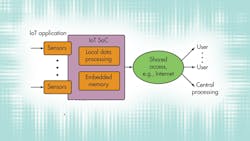
In all these applications, data is collected locally through various sensors. Some processing and data reduction are also performed, and the resulting information is then transmitted (Fig. 1). On the receiving side, data from several sources can be aggregated and further processed until meaningful information is generated and provided to the user through an additional service.
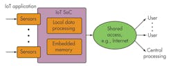
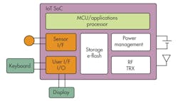
The device that performs these functions on the distributed side can be built around a system-on-chip (SoC) integrating a specifically designed applications processor for high-end applications or around a general-purpose MCU IC for low-end applications. In both cases, the device can be partitioned into a small number of functions: battery/power management, embedded flash (e-flash) memory, user interfaces (I/F) and other I/O, the wireless or wired (RF transceiver, TRX) communications interface, and the mission-critical sensor I/F (Fig. 2). Sensor devices are commonly divided into analog and digital categories.
The digital sensor outputs data in a digital format. It may already take care of some of the data processing, like calibration and other functions. Also, it may implement sensor fusion techniques by including several different sensors and combining them to derive meaningful information, as in motion detection.
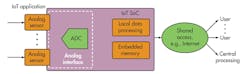
The analog sensor outputs raw data in analog format. There is a significant range of analog sensors such as temperature whose output is delivered in the analog domain. The application SoC needs to collect the output in raw format and convert it to digital for processing.
When connecting with a digital sensor device, the IoT SoC needs to include a digital interface that complies with the one the sensor chip is using to drive the sensor signals into the processor in the SoC. When connecting with an analog sensor, the IoT SoC needs to convert the sensor signal into the digital domain by means of an analog-to-digital converter (ADC).
Although an external ADC can be used, it is often more effective to implement an integrated ADC to reduce the printed-circuit board (PCB) footprint, which is critical for miniaturized applications such as wearable devices, as well as for cost reduction.
The interface to the IoT SoC is an analog port facing an integrated ADC (Fig. 3). Together with the sensor itself, the characteristics of this ADC often determine the ability to faithfully replicate the quantity being measured in the digital domain for further processing. When implementing an SoC for such applications, consider the tradeoffs involved in defining this analog interface.
Advantages Of An Integrated Analog Interface
Any IoT system needs to be able to support analog and digital sensors to be truly flexible. While a solution based on external ADC discrete components is functionally acceptable, the cost in terms of PCB real estate and bill of materials (BOM) can be prohibitive. That’s especially true for IoT systems that must be very small, particularly for wearable (textiles, etc.) and healthcare-related (intra-body or swallowable pills) devices.
The integration of an ADC with adequate performance has the potential to greatly simplify the design of the system and contribute to further energy efficiency for the total system, which is a critical criterion for remote battery-powered devices. Integrated ADCs save power because they eliminate the need for additional digital interfaces. They also are inherently low power and can be tightly integrated with the power management and control of the SoC.
For example, an integrated ADC can react very quickly to instructions coming in from the processor and then return to a power-saving idle mode. Alternatively, it can be made to acquire data autonomously while the processor is, itself, in idle mode and trigger processor operations on a certain simple criterion. It also can be slowed down or its supply level can be reduced to save power when speed is not needed. Even if some external ADC chips can support these power saving techniques, applying them to an integrated ADC is more effective due to its tighter integration with the SoC.
Performance Matters
Performance is the key parameter to consider when defining the ADC, but it’s important to understand which parameters are relevant for each application. In traditional sensor applications, for instance, the key criteria for the selection of the ADC would be linearity, which can be specified as differential and integral non-linearity. The sensor signal is expected to vary very slowly. The ability to sample at high speed with good dynamic performance, then, wasn’t usually required.
However, valuable information is included in the higher-frequency portions of some sensor signals. The dynamic performance of the ADC at these frequencies must be considered. Parameters like total harmonic distortion (THD) and signal-to-noise ratio (SNR) must be taken into account.
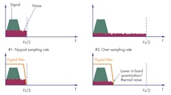
In some applications, the sensor signal being measured varies at very low frequency. Yet to obtain very accurate information about the dynamics of the signal, multiple harmonic components of the signal are acquired, resulting in the need to process signal bandwidths much wider than the actual signal. Other signals such as imaging and proximity detection may require processing of signals with even larger bandwidth.
In these applications, the minimum conversion rate is determined by the signal bandwidth, in accordance with sampling theory. However, it is often useful to have the ADC operate at higher sampling rates than the minimum necessary (Fig. 4). First, the in-band SNR of the system can be improved by oversampling the signal. Second, latency is reduced proportionally to sampling rate. Finally, additional channels can be sampled in the same time interval.
Minimizing The Impact Of SoC Integration
When considering the performance tradeoffs resulting from integration of the ADC in an IoT chip that also implements large signal processing blocks, the impact of noise coupling from the on-chip digital signal processing blocks in the ADC must be minimized.
Take, for example, a 12-bit converter that has to resolve signal amplitudes down to a least significant bit (LSB) of only 730 µV. It’s clear that noise immunity must be factored in because inside a digital integrated circuit, supply noise, and even substrate noise can easily surpass this amplitude and disrupt the operation of the converter. Noise isolation can be effectively addressed at several levels.
At the converter block level, circuit isolation techniques, differential topologies, and an internal low-dropout regulator (LDO) can be used to improve supply noise rejection in critical blocks. Other possibilities like the use of a deep-Nwell process option also can improve isolation, though these process options impact fabrication cost and typically are not used.
Careful signal and supply distribution and isolation can be used at the integration level. Internal LDOs effectively increase the supply rejection of critical elements in the circuit, reducing the overall sensitivity to noise.
At the system level, specific operation modes may be defined to reduce the noise to its minimum. For instance, several samples can be averaged to serve as an effective low-pass filter for any type of white noise that may be present in the input signal or be coupled in other elements of the signal processing chain. In cases where maximum accuracy is needed in a single-shot acquisition, the system can be stopped (or its activity reduced) during the critical sampling instant.
Integrated Features Are Important In The ADC
Besides raw performance, integrated features can make the difference in terms of how useful the ADC is. For example, an integrated multiplexer with as large a number of inputs as possible enables interfacing with multiple sensors. Applications such as temperature sensing may require the readout of different sensors. The ability to acquire them with the same converter can simplify the system design.
Also, support for single-ended and differential signals enables direct interfacing with different types of sensors. Sensors can generate either of the two different types of signaling, so support for both types of signals is important.
Compatibility with the wide range of signals with different amplitudes that sensors produce enables exploration of the full performance of the ADC. The dynamic range of the ADC input should match the dynamic range of the signal (Fig. 5). This can be achieved by several means, including implementing gain control at the input of the ADC with a programmable gain amplifier (PGA) and implementing gain control by adjusting the reference voltage for the ADC, which defines the dynamic range of the ADC.
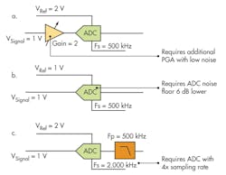
Furthermore, allowing the input signal to explore only a sub-range of the total ADC input voltage range and implementing gain in the digital domain results in lower SNR. However, this can easily be recovered through oversampling.
Allowing a wide supply range enables the IoT device to operate while the battery is being discharged. It also reduces the voltage level and extends the effective life of the battery.
Finally, the calibration of offset and possibly gain enables absolute accuracy. In cases where good integral non-linearity (INL) and differential non-linearity (DNL) characteristics are not enough, offset and gain errors should be minimized. Embedded calibration circuitry is very effective and greatly simplifies the task of obtaining accurate transfer functions for the ADC.
Other features such as a built-in temperature sensor, built-in reference generator, or dedicated regulator can simplify usage of the ADC in real applications as well.
Need To Keep Costs Down
System cost is important to consider when deciding whether to integrate the interface for analog sensors into the IoT chip. Integration contributes to cost reduction by reducing BOM by eliminating or reducing the need for external components. It also reduces total system area requirements, since PCB real estate is critical in most applications.
Additionally, the IoT chip itself requires an ADC function for its internal “housekeeping” purposes. The chip typically includes a range of internal sensors for temperature, battery voltage, and more. Some of the multiplexed inputs of the ADC can be dedicated to these purposes.
By sharing the same embedded resource, the system implementation becomes more area efficient, reducing its cost. In fact, since the integrated ADC functionality is required for internal purposes in any case, it can be argued that integrating the analog sensor interface has a negligible impact on the silicon area.
Conclusion
IoT applications are generating a lot of attention from the industry and from consumers. The interface with the sensor is a key element of the system that can benefit from integration. Effective analog sensor interfaces for IoT applications can be integrated to reduce costs and save power without compromising the flexibility of the system.
Today’s system integrators have access to a wide range of data converter IP created specifically for integration with digital processing blocks for sensor-based applications. This IP offers the range of performance and functionality that matches the characteristics of most sensors. Furthermore, they address critical system-level requirements such as BOM reduction and power conservation, yielding a more efficient system.
Reference
“Fridge sends spam emails as attack hits smart gadgets,” www.bbc.com/news/technology-25780908
Manuel Mota, technical marketing manager for analog intellectual property (IP) within the Solutions Group at Synopsys, has worked in the semiconductor industry for more than 10 years as an analog IP designer for Chipidea Microelectronica (Portugal) with responsibility for the design of phase-locked loop (PLL) and data conversion IP cores as well as complete analog front ends for communications. He later assumed the role of business developer for data conversion products with the responsibility of product definition and pre-sales technical engagement with customers. He joined Synopsys from MIPS Technologies in May 2009, assuming the technical marketing manager role. He holds a PhD in electronic engineering from the Lisbon Technical University, which he completed while working at CERN (Switzerland) as a Research Fellow. He has authored several technical papers and presented at technical conferences on analog and mixed-signal design.
About the Author
Manuel Mota
Senior Manager, Product Management, Die-to-Die IP, Synopsys
Manuel Mota is currently Senior Manager of Product Management for Die-to-Die IP at Synopsys. He holds a Ph.D in electronic engineering from Lisbon Technical University and has held research and technical positions at The European Organization for Nuclear Research (CERN) in Geneva, Chipidea, and MIPS.
Comment About the Article
To join the conversation, and become an exclusive member of Electronic Design, create an account today!

Leaders relevant to this article: