Dither Can Boost Sampled Data System Performance By At Least 10 dB
Sample rates for analog-to-digital converters (ADCs) and digital-to-analog converters (DACs) continue to evolve, now reaching 5 Gsamples/s at 10-bit resolutions and 1.5 Gsamples/s at 12 bits. These devices have traditionally fallen within the province of the military, where applications such as radar and electronic countermeasures require high sampling rates and large bandwidths.
Today, however, such performance levels have spread into several other markets. Examples include test instrumentation (oscilloscopes, spectrum analyzers), comercial off-the-shelf (COTS) board manufacturers, semiconductor automatic test equipment (ATE), high-speed hard-disk test equipment, and laser distance measurement systems.
Frequency-domain applications such as direct downconversion receivers are becoming a well-established arena for ADCs. Direct generation of transmission signals and direct conversion of received signals without external downconversion mixers is no doubt attractive, offering the advantages of flexibility and reduced component count.
Despite the “state of the art” of these converters, certain applications require still higher performance such as basestation design and signal synthesis. That’s why designers will consider adding signal-processing techniques in the digital domain, e.g., lookup-table correction, averaging, and dither signals, to significantly improve the performance of a sampled data system.
What Is Dither?
Dither is defined as the addition of an externally applied disturbance to the intended signal prior to digitization. In essence, it spreads the effect of the signal’s interaction with the measurement system, reducing the measurement system’s imperfections.
The dither technique has seen extensive use in enhancing audio quality. It’s also used in control systems to alleviate the effects of nonlinearity, hysteresis, and static friction, as well as in instrumentation systems.
Dither should be uncorrelated in time, uncorrelated with the analog signal, and constant in amplitude. The level of the dither should be judged with respect to the level of spurious interference that it’s due to reduce.
The dither signal can have different forms: triangular dither, sinusoidal dither, uniform, or Gaussian dither. Each presents a different attribute in the system’s performance.1
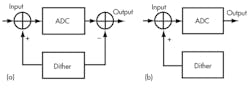
The dither technique typically takes on one of two basic arrangements: non-subtractive or subtractive (Fig. 1). For the subtractive arrangement, both the analog and the digital versions of the dither signal must be available. This is easy to fulfill in case of digitally generated dither. Here, a DAC can provide the dither signal and the input word can be subtracted from the input. Non-subtractive dither is generally employed in the frequency domain in an unused part of the spectrum, allowing a dither signal to be utilized and then filtered.
Dither Effects In ADCs
Quantization
The ADC quantization process introduces an error in the output signal with respect to the analog signal. This error is a function of the width of the quantization step. The error can be transformed into a noise value with the formula:
VNOISE RMS = q/√12
where q is the width of the converter’s least significant bit (LSB).
From this, the ideal signal-to-noise ratio (SNR) for a data converter can be derived:
SNR = 6.02 × N + 1.76 dB
where N is the number of bits of the converter.
If a low-level signal of 1-LSB amplitude is input to an ADC, then the resulting digitization will yield a square wave with a duty cycle dependent on the offset of the signal about the LSB’s threshold.
If another dither signal were added to the noise, the output signal would toggle more frequently, reducing the harmonic distortion. If some time averaging also were used, it could increase the resolution. It’s important to note that adding dither would also impact the output signal’s overall noise level.
Increasing Resolution
If the ADC were perfect, with no additional input noise, the best resolution possible would be limited to the width of one LSB. However, adding some noise and averaging two measurement results could increase resolution by a factor of 3 dB. Averaging more samples would provide greater resolution at the expense of effective sample rate.
Oversampling is one way to avoid throughput loss caused by averaging. With every factor of 2 in the oversample rate, the system would gain an extra one-half bit in resolution.
High-resolution ADCs generally have some input-referred noise. This means that for a perfectly noise-free input, the output would not be one fixed code. This can be useful when there’s a need for higher resolution and averaging can be employed.
Improving Linearity
In low-speed ADCs, linearity is characterized by integral nonlinearity (INL) and differential nonlinearity (DNL). INL is the maximum deviation of the ADC’s response to the best-fitting straight-line plot, while DNL represents the maximum difference in the size of an LSB.
For high-speed ADCs, a more commonly used parameter for linearity is spurious-free dynamic range (SFDR). It’s the ratio of the rms signal amplitude to the rms value of the highest spurious spectral component. SFDR is commonly used because it directly indicates the effect of INL on the output signal in the frequency domain.
For the most part, two sources influence SFDR: the nonlinearity of the front-end track-and-hold amplifier and preamplifier, and the nonlinearity of the ADC core. The latter is typically due to mismatches in the resistance ladder and comparator circuits.
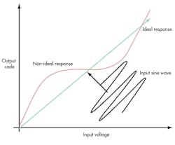
Some correlation exists between quantization noise and input signal that can affect SFDR. However, it’s generally of a lower level in high-speed ADCs (Fig. 2).
Low SFDR in an ADC is desirable because it plays a role in direct-conversion applications. For example, when there’s a large interfering signal in the same band as a lower-power signal of interest, harmonics from the interferer could affect demodulation of the wanted signal. Also, in radar systems, harmonic spurs could be misinterpreted as targets, degrading system performance.
Methods Of Adding Dither
One of the most common sources of white Gaussian noise is the reverse-biased diode. The quantum mechanical nature of the electron-hole paring process produces a truly random noise signal with very high bandwidth. The signal then can be amplified and filtered depending on measurement or application needs.
The pseudorandom bit stream (PRBS) offers another way to generate noise-like signals. This process generates a bit stream via a shift register containing feedback elements. The position and number of feedback elements in the shift-register array produces different length sequences, and the maximum-length sequences exhibit random noise-like behavior. The noise sequence can be filtered and amplified to produce the required noise pattern. This type of noise generation is ideal for subtractive noise generation. One drawback is that the clock frequency may limit noise bandwidth.
A high-speed DAC (described in the following section) also can generate noise. One advantage is that it allows for rapid modification of noise parameters. The DAC’s performance must be well above that of the ADC to produce reliable results, though.
In particle detection, the arrival of each particle is random. Therefore, it’s not always necessary to introduce a noise-like dither. Instead, all that’s needed is to add the input signal to a linear ramp and then subtract the ramp’s value from the output signal. This technique has been used in time-to-digital converters and particle amplitude instrumentation.
Determination Of Dither-Signal Parameters
It can be shown that the enhancement of resolution and linearity is equal for an ideal ADC and can be evaluated with the equation:
NEFF = N + ½ log 2(n/1+k2)
where N = number of bits, NEFF = effective number of bits after averaging, n = number of samples, and k = URMS 2(N+1)√3/FS. URMS is the value of added noise, and FS is the full scale of the ADC.2
There’s little effect if the dither amplitude is below the value of an LSB. Alternatively, a normally distributed random signal with an RMS value bigger than approximately 0.35 qcan be used (q = width of LSB).2 One caution: Adding too much dither to a sampled data system can cause the device to saturate, which will increase the harmonics.
In subtractive dither systems, the ability to completely cancel the added noise is important. A slight mismatch between the added and subtracted noise results in an incomplete cancellation. The larger the added noise, the worse the effect of this incomplete cancellation. This is one of the main reasons for limiting the amount of added noise.
Practical Examples
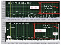
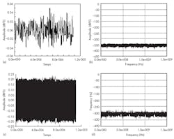
A high-speed 12-bit converter developed by e2v, the EV12AS200, comprises a single-core 1.5-Gsample/s ADC with 2.3-GHz bandwidth.3 It’s based on a 200-GHz silicon-germanium-carbon (SiGeC) bipolar technology. In L-Band radar applications, the device enables direct digitizion of 500-MHz broadband arbitrary waveforms in the second Nyquist region closer to the antenna—a key factor when designing flexible, simplified radar receiver systems.
Adding dither to the EV12AS200’s input signal will enhance performance. This was demonstrated in a test using a filtered noise diode as the dither source input to one side of the ADC’s differential input (Fig. 3).
Dither Effects On High-Speed DACs
All of the features discussed to this point also apply to DACs. The difference lies in the methods of pattern generation and in their application.
High-speed DACs are typically found in military electronic warfare systems, automatic test systems, waveform synthesis, and communication systems. Such DACs also can be employed at slightly lower frequencies in cable drive applications, such as those highlighted by the DOCSIS standard. These systems require extremely low SFDR, some greater than −80 dBc.
A multiplexed bus often acts as the interface to high-speed DACs. It enables reduction of the individual bit rate for each port in line with the common FPGA rates.
Generate Test Patterns
Standard static testing doesn’t apply to high-speed DACs. Ideally, the DAC should be tested at its frequency of use, since DAC performance can change at higher frequencies. In general, spreadsheet macros, C code, or dedicated signal-analysis software is used to produce the DAC’s test vectors. The software is the most user-friendly.
Test patterns are required for all characterization testing of these devices. Typically, they involve single-tone measurements; dual- or multi-tone signals; adjacent channel power ratio (ACPR) signals where there’s generation of random quadrature-amplitude-modulation (QAM) signals within a particular channel; and noise power ratio signals where broadband random noise is generated with a notch around certain frequencies.
Frequency should be carefully generated for single-tone patterns, making sure that the waveform has an integer number of cycles within the record length. This ensures that there’s no spectral leakage. The formula to follow is:
FOUT/FSAMPLE = N of cycles/N of samples
where FOUT is the required output frequency; FSAMPLE is the sample rate of the DAC; N of cycles is the number of cycles in the pattern (this should be a prime number to ensure that there are no repeated identical code sequences); and N of samples is the number of points in the pattern (this should be a multiple of 2).
Generating the pattern in the time domain involves repetitive sampling techniques. The sine-wave generator steps each sample it produces forward in phase by a small increment. This will ensure that all codes are produced in the test sequence.
Noise Generation For Dither
When using dither with high-speed DACs, a dither signal that’s generated in the digital domain must be added to the required signal. Because the DAC will generally be part of the transmission system, non-subtractive dither will most likely be employed. Typical methods for generating a dither signal include:
- A random-number generator followed by a high-order finite impulse response filter in the time domain.
- Application of a white Gaussian noise waveform, transformed to the frequency domain, filtered, and then inverse Fourier transformed back to the time domain.
- Use of different phases of a sinusoid in each frequency bin, which are subsequently transformed back to the time domain.
The noise generators can be based on already available software functions and are modifiable to produce the distribution required. One flexible and convenient way to generate and modify DAC test patterns is to use a graphical analysis tool such as SILAB (Fig. 4).
DDS System Dither
Direct-digital-synthesis (DDS) systems, phase-locked to an external clock, generate high-quality analog signals using a digitally defined frequency. They’re used in systems such as radar and electronic warfare systems, as well as agile communications systems that require small-step frequency changes and extremely fast hopping speeds.
The common structure uses a DAC output. It’s preceded by a digital block called a phase accumulator, which produces the digital sinusoidal pattern. A large word size is needed to produce the low-hertz step size. Ultimately, the phase accumulator outputs to a sine lookup table.
The large word size of the phase accumulator means that the word output to the DAC must be truncated to fit the limits of the DAC’s input. This truncation leads to small discontinuities in the generated pattern, creating greater harmonic distortion. Using dither in the generation of the phase accumulator output can reduce these “truncation spurs.”
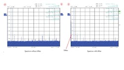
For example, the EV12DS130A is a 12-bit, 3-Gsample/s DAC with special output-pulse-shaping techniques that reduce SFDR values to less than 70 dB.4 With its 7-GHz output bandwidth, the DAC can upconvert signals at microwave frequencies. Previously, multiple up-mixers would have been required. Now they can be deleted along with the accompanying VCO/PLL jitter that adds at every upconversion. Added dither is a good thing because it can be subtracted since it is known. Jitter is not known so cannot be subtracted. Some tests illustrate the potential increase in performance with deliberately added jitter (Fig. 5).
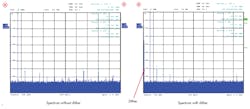
The first plot in the figure shows a test pattern of 100 MHz that establishes baseline performance; spurious levels are already well below −70 dBc. In the second plot, dither, at an amplitude of −20 dBFS, was added. Spurious signals at higher frequencies are gone. The remaining spurious signals are attributed to phase imbalance of the output balun and spectrum-analyzer spurious performance.
References:
- R. Wannamaker, “The Theory of Dithered Quantization,” PhD thesis, Department of Applied Mathematics, University of Waterloo, Waterloo, Ontario, Canada, July 1997.
- J. Holub, O. Aumala, “Data Processing and dither enhancement of ADC parameters – Trends, Applications, Limits,” IMEKO TC4 2002-009.
- M. Wingender, et al., “12 Bit 1.5 GS/s L-Band ADC on 200 GHz SiGeC Technology,” IEEE Conference Radar 2011, Cheng-du, China.
- F. Bore, et al., “3 GS/s 7 GHz BW 12 Bit MuxDAC for Direct Microwave Signal Generation over L, S or C Bands,” IEEE International Conference on Microwaves, Communications, Antennas and Electronic Systems 2011, Tel Aviv, Israel.
Andrew Glascott-Jones is an applications engineer for e2v’s mixed-signal ASICs business unit in Grenoble, France. He brings 25 years of experience to his position as an applications engineer within e2v’s mixed-signal ASICs business unit. His specific area of expertise lies in the design of electronic measuring systems, including precision metrology, particle sizing, X-ray imaging and laser spectroscopy.
Contributors
O. Bonnet, F. Bore, V. Monier, and M. Wingender
About the Author
Comment About the Article
To join the conversation, and become an exclusive member of Electronic Design, create an account today!

Leaders relevant to this article: