Dual Comparators Match Precision Industrial, Instrumentation Application Needs
This file type includes high resolution graphics and schematics when applicable.
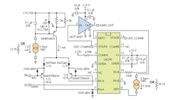
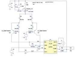
Dual precision comparators are needed in many designs, such as for industrial and instrumentation applications, to generate accurate pulse-width modulated (PWM) waveforms with very high (>99%) and very low (<1%) duty-cycle percentages. This design idea (Fig. 1) improves on designs based on the common LM311 and LT1011 devices, both of which require resistor pull-ups and have asymmetric timing paths. The features of this new design include matched, short propagation delays (Tpd); accurate duty-cycle generation; push-pull, rail-to-rail output; and operation from a supply above 15 V.
The circuit is based on the LM359 high-speed video op amp with an additional bipolar PNP input stage, and an MCP1402T output driver powered with a single +15-V supply. The LM359 is used to get a high-speed “IC Process” device to meet a comparator’s specifications. This IC also permits design changes at a low level because it has both input and output programming-current pins, and the compensation node is available as well. Input and output programming currents are driven by a 0.5-mA source.
Since this op amp is a dual device, one half is connected as a comparator and the other half remains as a spare. A spare is shown to define its connections. A transconductance stage is placed ahead of the LM359’s current-mode input to enable a voltage-mode input. The gain is reduced at the cascade stage’s high-impedance node (COMP pin) by the 4.99-kΩ resistor. A capacitor in parallel with the resistor also controls the bandwidth of the LM359. The IN- terminal of the LM359 is an additional high-impedance node and it, too, can be locally compensated to GND. (Figure 43 of the LM359 datasheet, "Adding a JFET Input Stage," helped spark ideas for the input stage.)
The output of the LM359 is connected to the input of the MCP1402T, a device that can drive rail-to-rail and drive capacitive loads very well. The LM359’s supply voltage can even be set to a lower voltage level and the MCP1402T can still be set to drive to a 15-V output level. The maximum supply voltage of the comparator is limited by the MCP1402T to 20 V dc, which means that is can be used for 18-V designs.
Using a higher supply voltage improves signal-to-noise ratio (SNR), as there is a larger signal for a given amount of noise. Also, large input signals dominate any voltage-offset terms, which is an advantage of using the higher voltage supply. (Note that the output polarity can also be easily changed on a fabricated printed-circuit board by using a MCP1401T in place of the MCP1402T.)
The circuit uses both 1-mA and 0.5-mA (two-terminal) current sources. In the original design, custom sources were used, but resistors can be used in their place (although with a reduction in supply rejection performance). An LM334 is also an option, as well as a JFET with a source resistor to control VGS. The 1-mA current biases the SIR19-21C/TR8 IR LED; a 1.2-V shunt voltage reference can be used in place of the IR LED. The 1N4148W diodes at the transconductance input stage protect against reverse-biasing at the emitter-base junctions, while the BAT54A prevents current from one side or the other of the differential pair adding to the tail current.
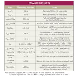
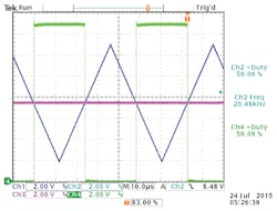
The table shows the measured results of this circuit, and Figure 2 shows measurements of key nodes in the comparator and the matching of both comparators. The measured propagation-delay mismatch causes the 0.06% offset from 50% duty cycle. Several simulations were also done for this circuit, using the Spice circuit of Figure 3 to simulate systematic VOS and IIN over the input-voltage range.
Tim Davis graduated with a BSEE from Iowa State University in Ames, Iowa. He has more than 28 years of experience in analog circuit design, power electronics, and IC design, including several patents for electronics in the medical industry. He can be reached at [email protected].
About the Author
Tim Davis
Engineer
Tim Davis graduated with a BSEE from Iowa State University in Ames, Iowa. He has more than 28 years of experience in analog circuit design, power electronics, and IC design, including several patents for electronics in the medical industry. He can be reached at [email protected].
Comment About the Article
To join the conversation, and become an exclusive member of Electronic Design, create an account today!

Leaders relevant to this article: