Faster JESD204B Standard Presents Verification Challenges
This file type includes high resolution graphics and schematics.
JESD204B is a new 12.5-Gbit/s serial interface standard for high-speed, high-resolution data converters. Already, devices from converter manufacturers are beginning to make their way into the market, and the number of JESD204B-enabled products is expected to increase tremendously in the near future. The primary value of the JESD204B interface is a reliable increase in the data transfer bandwidth between a converter and a logic device such as an FPGA or ASIC.
As with any new interface, JESD204B brings new challenges. For system developers, the challenges are how to best implement JESD204B from a printed-circuit board (PCB) design standpoint and how to debug a system if something isn’t initially working right. For component manufacturers, challenges involve testing new JESD204B devices. Testing not only ensures that specifications are being met in a relatively ideal environment, it also ensures successful JESD204B operation in end system environments.
A Natural Evolution
Data converters (digital-to-analog and analog-to-digital) are used in many applications ranging from audio and music to test instrumentation. The world of data converters is evolving. As the bit depth and sample rate go up, it is becoming more and more difficult to get data in and out.
A decade or two ago, with sample rates for high-speed converters limited to 100 Msamples/s and below, using transistor-transistor logic (TTL) or CMOS parallel data busses was sufficient. For example, a 12-bit converter with 12 pins dedicated to data could be implemented with reasonable setup and hold times with respect to the clock.
As speeds increased above 100 Msamples/s, setup and hold times for single-ended signals no longer could be maintained. To boost speeds, high-speed converters moved to differential signaling, but at the cost of increased pin counts. For example, a 12-bit converter now would need 24 pins dedicated to data.
To address the pin count issue, serial data interfaces were adopted. A converter data interface with 6x serialization now allows that same 12-bit converter to transfer data with just two differential I/Os (only four pins). Fast forwarding to today, data converters are now being developed using the JESD204B specification for the data interface.
The JEDEC standards organization has published two versions of the JESD204 high-speed serial digital interface specification. The first, JESD204 2006, brought the advantages of SERDES-based (serializer-deserializer) high-speed serial interfaces to data converters with a 3.125-Gbit/s maximum speed rating. It was revised in 2008 (JESD204A 2008), adding important enhancements including support for multiple data lanes and lane synchronization.
Comprising about 65 members from 25 companies, the international JEDEC JC-16 Task Group (Project 150.01) developed the second version of the specification, JESD204B.1 Its major enhancements included a higher maximum lane rate, support for deterministic latency through the interface, and support for harmonic frame clocking.
Lack Of An Official Compliance Test Specification
Unlike many other high-speed serial interface standards, JESD204B doesn’t include an official compliance test specification. A test specification is doubly valuable because it lists the tests that must be performed to ensure compatibility as well as the procedures for doing those tests. Consistent procedures used by different manufacturers helps ensure a common understanding of the specification and eliminate differences in assumptions.
The lack of an official compliance test specification does not mean all is lost, though. All of the information needed to develop a set of tests and procedures can be found in the JESD204B specification and the specifications it refers to. Individual chip manufacturers and system developers must pull together that information.
PHY Testing
Physical-layer (PHY) tests are related to the individual data lane driver and receiver circuitry—in other words, the analog tests of a link. They do not include digital functionality or procedural tests. Working toward the development of a thorough list of PHY tests, a list of recommended SERDES PHY tests can be obtained from the OIF-CEI-02.02 specification, section 1.7.
The JESD204B specification closely follows those recommendations, but it does include a few modifications. For example, JESD204B does not specify random jitter as a standalone test item, including it under total jitter instead. Also, JESD204B specifies JSPAT, JTSPAT, and modified RPAT as recommended test patterns whereas OIF-CEI-02.0 specifies using the PRBS31 pattern.
Above and beyond the required PHY tests, additional PHY tests that aren’t listed in OIF-CEI-02.0 or in the PHY section of the JESD204B specification could be performed. One can look to other SERDES compliance test specifications for examples and find tests such as intra-pair skew (for a Tx) and intra-pair skew tolerance (for an Rx).
These tests don’t necessarily need to be added to the JESD204B specification, though. Additional PHY tests are not required to ensure JESD204B compatibility. But if a particular PHY test is failing, other PHY tests can be used to help gain insight as to why.
Once the list of tests is set, limits for those tests can be obtained from the JESD204B specification. Just keep in mind that there are three sets of limits, LV-OIF-11G-SR, LV-OIF-6G-SR, and LV-OIF-SxI5. A particular JESD204B device may support more than one set of limits. In that case, the component should be tested against all of the supported sets of limits.
1. Jitter represents a potential point of confusion for JESD204B testing as terminology varies in the standards documents provided by OIF compared to terms used in standard Dual-Dirac jitter models from Tektronix (that now includes bounded uncorrelated jitter as shown) and other test equipment vendors. The table provides a handy translation of those terms.
One point of potential confusion with JESD204B PHY testing is jitter terminology. JESD204B and OIF-CEI-02.0 use different terminology from what the test equipment vendors use (Fig. 1). Test equipment makers base their terminology on the industry standard Dual-Dirac jitter model. This difference in terminology is a point of potential problems in test procedures, as jitter is a quite tricky topic (see the table).

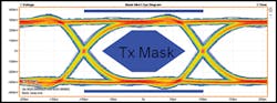
Another point of potential confusion with JESD204B PHY testing is the eye mask for data rates above 11.1 Gbits/s. The JESD204B specification says that for data rates greater than 11.1 Gbits/s, a normalized bit time of 11.1 Gbits/s should be used. So if you’re running at 12.5 Gbits/s (with an 80-ps bit period), the bit period for 11.1 Gbits/s (90.9 ps) should be used.
The issue at hand here is that eye masks can be built by starting either at the edge of the user interface (UI) or from the center of the UI, and the JESD204B does not clearly state which reference point to start from. If the reference point is the center of the UI, then the eye mask is bigger than normal at 12.5 Gbits/s, making it harder for a Tx to pass but easier for an Rx to work. If the reference point is the edge of the UI, then the eye mask is smaller than normal at 12.5 Gbits/s, making it easier for a Tx to pass but hard for an Rx to work. Ultimately, until this question is resolved, you should test against each of the two mask options to ensure compatibility.
Timing Testing
Coming up with a thorough list of timing tests for JESD204B is not an easy task. There are at least a dozen timing diagrams throughout the specification and it’s not immediately apparent which apply to the Tx, the channel, or the Rx. Also, some only apply to a particular subclass (0, 1, or 2). An official compliance test specification would be especially helpful here if it were to simply consolidate the timing specifications into a single table. Once time is taken to methodically go through the timing specifications, there is no confusion about them.
One nice thing about timing for system developers is that specifying timing for a JESD204B component turns out to be easier than is immediately apparent from the specification. For subclass 0 and 2, only Device Clock-to-SYNC~ timing must be specified. For subclass 1, only Device Clock-to-SYSREF timing must be specified.
Protocol Testing
As with the PHY tests, there is no official list of JESD204B protocol tests. Therefore, each user must scour through the specification and compile a list of functions to test. For example, the test sequences are one category of protocol tests.
For PHY testing, JESD204B transmitters must be able to output JSPAT and modified RPAT patterns. From a protocol standpoint, there’s a need to validate that those patterns are correct. The same is true with JESD204B receivers and the JTSPAT pattern. Optionally, if they support PRBS patterns, those need to be validated as well.
Next, the short and long transport layer patterns are included to help system developers debug their systems by proving that the link is working correctly through the transport layer. From a component manufacturer standpoint, those transport layer patterns have to be validated for every mode of operation that the device supports, which, considering the number of link configuration variables, ends up being a lot of cases.
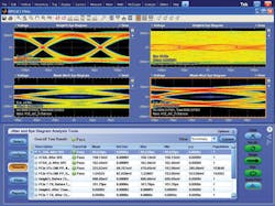
One question that comes up regarding protocol testing is how to do it at 12.5 Gbits/s. One recommended solution is to use a high-speed oscilloscope with a serial data decoder. Many higher-end oscilloscopes are now equipped with a dedicated trigger chip for triggering on 8b/10b data such as that used in JESD204B (Fig. 2).
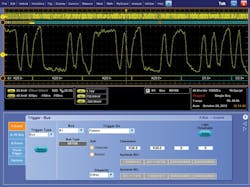
2. Today’s performance oscilloscopes are equipped to decode incoming waveforms to display 8b/10b data such as that used in JESD204B. This Tektronix oscilloscope is performing a serial decode of a JESD204B data lane at 6 Gbits/s at the beginning of the initial lane alignment sequence (ILAS).
Another group of protocol tests can be built around the initial lane alignment sequence (ILAS). The ILAS as a whole is fairly complex, so breaking it down into its individual components can make protocol testing more meaningful. Some tests can be measured on a transmitter to validate its operation.
For example, is the multiframe length correct? Does each multiframe start with a /R/ control code and end with a /A/ control code? Is the /Q/ control code in the right location? Is the link configuration data correct and in the right location? Does the ILAS contain data? How many multiframes does the ILAS last? Is the ILAS the same on all lanes? Clearly, there is a lot of potential for protocol testing around the ILAS sequence.
JESD204B does not have a lot of handshaking, but what it does have can be tested. Depending on the subclass, a number of tests can be performed. Since the SYNC~ signal can be used for initial handshaking, error reporting, and link re-initialization, do the Tx and Rx components do their part accordingly? Does the Rx assert SYNC~ starting at the right time and for the right duration? Does the Tx react correctly based on the duration of SYNC~ assertion? Since the data sent over the link also plays a part in the handshaking (i.e., the ILAS), is it correct for its content and with respect to SYNC~ timing?
Next, some smaller digital functions need to be tested as a part of protocol including scrambling, 8b/10b encoding/decoding, skew and skew tolerance, control bits, tail bits, SYNC~ signal combining, frame alignment monitoring, and correction. All of these functions need to be validated.
Lastly, there is the error handling category of protocol tests. The specification includes a minimum set of errors that must be detected and reported: disparity errors, not-in-table errors, unexpected control character errors, and code group synchronization errors, but many more potential errors could be detected and reported. For each and every type that is detectable by a JESD204B component, there should be a protocol test.
These types of protocol tests can be a bit of a challenge to test and validate because a properly working link will never exercise them. They generally will require specialized test equipment. A bit error rate test (BERT) pattern generator can be used for many tests by creating a pattern that includes an error. Error cases can also be generated using an FPGA with code modified to specifically generate those errors.
Emphasis And Equalization Testing
The JESD204B specification covers very little about emphasis and equalization. There are a few comments like “pre-emphasis might be required” and “equalization might need to be implemented,” from which one can determine that the specification allows them but does not give any additional guidance.
When using a converter with JESD204B that includes emphasis or equalization, how does one go about determining whether or not to turn it on and, if so, how much to turn it on? To answer that question, it is first best to understand the type of jitter called inter-symbol interference (ISI), which is the name for the variation in edge timing caused by the filtering effects of a transmission line.
Mathematically, ISI can be simply modeled as a low pass filter. When sending high-speed serial data down a transmission line, the filtering results in a distorted signal. Emphasis and equalization counteract the filtering effects of ISI with the goal of bringing the frequency response at the end of the channel back to as close to flat over frequency as possible, resulting in a signal that isn’t distorted by ISI.
With a basic understanding of emphasis and equalization and ISI, the next step is setting them. Many people first ask how long of a trace can be driven with and without emphasis and equalization. Real-world PCB designs have too many variables that can affect ISI to be able to specify the channel in terms of trace length.
Variables like trace width, trace length, vias versus no vias, dielectric material, connectors versus no connectors, trace material, corners, passive components, and distance to ground plane can all affect channel performance. So how can channel characteristics ever be correlated to emphasis/equalization?
The solution is to specify the channel in terms of insertion loss, which JESD204B describes as a measure of the power loss of a signal over frequency. Emphasis, equalization, and PCB channel can all be related in terms of insertion loss (and gain). Using a relevant frequency (JESD204B lists three-quarters baud rate) and an insertion loss limit (JESD204B lists –6 dB), the gain provided by emphasis and/or equalization can be selected to bring the frequency response at the selected frequency up above the loss limit. For example, a PCB channel with –12 dB of loss at 9 GHz would need +6 dB of emphasis and equalization gain to bring the total back up to –6 dB.
Alternately, converter manufacturers can provide a table of emphasis/equalization settings versus PCB insertion loss. This method can result in a better solution, as it does not depend on as many assumptions. To build such a table for a transmitter (and to emulate end system designs), a set of test evaluation boards can be built with varying trace lengths.
The eye diagram at the end of the PCB trace can be directly measured and compared against the JESD204B Rx mask. By trying various PCB trace lengths, one will result in the eye just barely passing the Rx mask. Since the insertion loss of that specific trace can be measured, the drive capability for a specific emphasis setting is known.
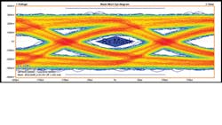
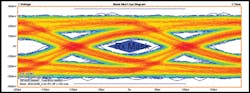
Compare Figure 3 showing an eye diagram at the end of an ISI PCB to Figure 4, the eye diagram going into an ISI PCB. In this case, the data rate is 5 Gbits/s, the ISI PCB has 8 dB of insertion loss at 4 GHz, and emphasis is off.
3. The eye diagram at the end of an ISI PCB trace can be directly measured by an oscilloscope and compared against the JESD204B Rx mask to determine if there are unacceptable levels of insertion loss. Compare this nearly closed eye to the one in Figure 4.
4. Eye diagram mask measurements enable you to compare insertion loss from different PCB trace lengths. See Figure 3 for a higher degree of insertion loss leading to a closed eye diagram compared to this eye going into an ISI PCB.
Repeating this process versus emphasis settings will result in a table of emphasis settings versus insertion loss. A similar approach can be taken on a receiver with equalization. Start with a BERT generator that is outputting the maximum allowed total jitter (except for ISI jitter). Using the same set of ISI test boards with varying trace lengths, test with longer and longer traces until the receiver starts to get errors that exceed the target bit error rate (1E-15). Measure the insertion loss of the PCB trace. Repeat for every equalizer setting.
In summary, if a JESD204B device manufacturer provides only emphasis/equalization gain, the first method can be used to pick settings. It’s best if the manufacturer provides a table of settings versus channel insertion loss.
Should you use emphasis or equalization? From a frequency response correction standpoint, there’s no clear reason to use one or the other. However, emphasis can generate a certain amount of gain with less power in most cases. If system power is important, that could be a reason to choose emphasis over equalization. Another advantage of choosing emphasis over equalization is that the effect on the signal can be directly measured with an oscilloscope.
Having both a JESD204B Tx with emphasis and an Rx with equalization can be common. How would you determine when to turn on both? Simply, if the insertion loss of the channel cannot be overcome by just emphasis or just equalization, then it’s time to turn on both.
As for how much gain to set each of them to, one advantage of specifying response in terms of insertion loss (and gain) is that it’s additive. For example, at the frequency of interest, a PCB trace with –20 dB of loss, a Tx with +6 dB of emphasis, and an Rx with +8 dB of equalization can be represented as –20 dB + 6 dB + 8 dB = –6 dB total.
Emulating System Environments: Noise And Jitter
No end system design is free of noise and jitter. JESD204B fully specifies system jitter emulation, but it doesn’t specify voltage noise. To emulate voltage noise in end system designs, component manufacturers can perform noise tolerance tests. One such test is power supply noise tolerance.
Noise is injected onto the components’ various power supply domains. The amplitude of the noise is increased until the first compliance tests fails. (Often the first test to fail on a SERDES will be jitter.) This test is repeated over the frequency range at which PCB noise is typically present (a few hertz to around 100 MHz). A plot of maximum power supply noise tolerated versus frequency is generated.
The same test can be performed on all other pins. The end result of all this testing is typically a set of practical PCB design recommendations, such as “keep a particular supply domain separated” or “use a bypass capacitor on this pin” or “don’t route any signals near this pin.”
Maintain Signal Integrity When Measuring
As with any high-speed serial test application, best practices apply to ensure accurate measurement results. Also, you must be sure that your instrumentation offers sufficient performance and signal integrity to deliver accurate measurement results. Considerations include:
• Dynamic range: In general, it’s best to use the full range of your oscilloscope’s analog-to-digital dynamic range without clipping the amplifier. Although clipping might be acceptable when looking at a clock signal, doing this will hide ISI issues when evaluating data signals. It also can affect the instrument’s edge interpolation algorithm.
• Sample rate: Setting the oscilloscope to the highest sample rate provides the best timing resolution for the most accurate signal and jitter measurement. One exception would be if you’re looking over longer time windows at lower timing accuracy.
• Capture window: Analyzing signals over a longer time window allows you to see low-frequency modulation effects like power supply coupling and spread-spectrum clocking. Increasing the capture window unfortunately increases the analysis processing time. On SERDES systems, there is often no need to look at modulation effects below the loop bandwidth of the CDR that are tracked and rejected.
• Test point access and de-embedding: Ensure that you employ a mechanism for keeping the probe as close to the Tx test point and as close to the Rx test point as possible. With high-speed signaling test, timing and amplitude measurements can seriously impact margin test results if the measurement process introduces unwanted signal discontinuity from long traces and/or fixturing from the actual Tx/Rx test points.
In some cases, the probe access point could be at a location where the signal is degraded due to the transmission line length. In this case, you might have to de-embed the transmission line to see what the real signal is. De-embedding involves recreating a model (using a linear method with S parameters) of the measurement channel between the instrument and the targeted test point. This model can be applied to acquired waveform data in the oscilloscope to account for transmission line degradations (Fig. 5).
5. By applying a model of the measurement channel to an acquired waveform, the effects of transmission line degradation can be removed or de-embedded for improved measurement accuracy. Tools like the Tektronix SDLA software shown here enable users to see the effects of model embedding and de-embedding.
By practicing good signal integrity in your measurement techniques, you’ll be better equipped to evaluate and characterize high-speed technologies like JESD2024B.
Summary
The recently released JESD204B interface can reliably increase data transfer bandwidth between a converter and a logic device, and new devices using this interface are making their way to market. Unlike many other high-speed serial interface standards, JESD204B does not include an official compliance test specification, creating a number of challenges for system designers who must thoroughly test and debug their designs. Fortunately, the specification includes sufficient information to develop testing procedures, including PHY, timing, and protocol tests.
In addition to validating performance and compliance with the specification, testing can help determine the need for emphasis or equalization in a system design and help to identify unwanted sources of noise and jitter. As with any high-speed serial testing effort, best practices for instrument selection, setup, and probing should be followed to ensure consistent and accurate results.
References
1. “Serial Interface for Data Converters, Document JESD204B.01,” http://www.jedec.org/standards-documents/results/taxonomy%3A2805, requires registration
2. “Implementation Agreement OIF-CEI-02.0,” http://www.oiforum.com/public/documents/OIF_CEI_02.0.pdf
Frank Farrelly is a product engineering manager at Analog Devices. He has been with the company for 19 years and is currently working on the characterization and validation of high-speed SERDES products. He holds a BSEE from the University of Tennessee, Knoxville, and an MBA from the University of North Carolina, Greensboro.
Chris Loberg is a senior technical marketing Manager at Tektronix responsible for oscilloscopes in the Americas Region. He has held various positions with Tektronix during his more than 13 years with the company, including marketing manager for Tektronix’s Optical Business Unit. His extensive background in technology marketing includes positions with Grass Valley Group and IBM. He earned an MBA in marketing from San Jose State University.
About the Author
Comment About the Article
To join the conversation, and become an exclusive member of Electronic Design, create an account today!

Leaders relevant to this article: