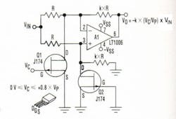
Op Amp And Two JFETs Form A Voltage-Controlled Amplifier
This article is part of the Ideas for Design in our Series Library
A simple linear voltage-controlled amplifier can be constructed with one op amp and two JFETs (see the figure). The amplifier can achieve an 80-dB dynamic control range with less than ±0.2% linearity error for 0 V ≤ VC ≤ 0.8 × VP.
R is chosen to be much larger than the RDS(ON) of the JFETs. This permits a large range of input voltages to be applied without driving the JFETs into a nonlinear region. If, for example, RDS(ON) = 100 Ω and R is chosen to be 10 kΩ , a 10-V input signal (VIN) will result in a VDS of less than 100 mV.
The value of k can be chosen to supply gain. Although p-channel JFETs are shown, n-channel JFETs will work as well for negative control voltages (VC). Also, it should be noted that the drain and source terminals are interchangeable in this application.
The JFETs should be chosen for low RDS(ON) and high IDSS. If a forward gate voltage is possible, a current limiter in the gate is advisable.
For the largest dynamic range, the resistor connected from VIN to the noninverting input can be adjusted for a minimum output with VC = 0 V. The trim range is about ±5% of R. For the lowest temperature sensitivity, maintain good thermal coupling between Q1 and Q2.
If VC = VIN, the circuit will perform as a voltage squaring circuit where VO = —(k/VP) × VIN2 for unipolar VIN (quadrant 4 for p-JFET and quadrant 2 for n-JFET).
About the Author

Henry Santana
Henry Santa is a senior engineer and registered professional engineer in Colorado. He received a BSEE from Colorado State University, Fort Collins.
Voice Your Opinion!
To join the conversation, and become an exclusive member of Electronic Design, create an account today!

Leaders relevant to this article:

