Passive Components Aren’t Really So Passive (Part 3): PCBs

Sometimes the best way to hide something is in plain view. Magicians use this technique along with some distraction to amaze an audience. Our experience leads us to expect certain norms and see what we expect. Thus, boxes are square, not squished parallelograms. Spheres are symmetrical, not hemispheres with elongated portions behind them.
In that same sense, printed-circuit boards (PCBs) seem straightforward. You think you can see everything going on, but you are really only looking at the circuitry on the exterior surface. In fact, if you delve deep enough down to the board itself, you find complex layers and structures and myriad things that can go wrong there.
When high-precision op amps and high-resolution data converters fail to perform as expected, we need to closely examine all the surrounding active and passive components, including the PCB. Into this context we also insert the PCB vendor and its understated role that is, in fact, critical for IC performance.
PCB flaws and errors that are usually hidden, or at least disguised, can introduce passive errors into IC performance. To understand how these errors occur, though, we must first examine the composition of a typical board. Four examples of PCB problems and efforts to solve those hidden errors will help us appreciate the contribution that a good, reliable PCB vendor makes to successful products.
This file type includes high resolution graphics and schematics when applicapable.
Passive Viewing—Seeing What We Expect
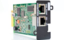
When you look at a typical board directly, what do you see (Fig. 1)? Perhaps you see an Ethernet connector and another RJ-45 connector with the labels “settings sensor,” “UPS data,” and “RS-232.” You also may see an inductor and electrolytic capacitors for a switching supply, several large-scale ICs, and a bunch of decoupling capacitors. Put all this together, and it probably is a digital board with several options because we can also see unstuffed components. Right? Yes, but we did not really see the bare PCB itself, and that is where this story starts.
Many things can go wrong with something as complex as a PCB. A good, reliable PCB vendor is very important. There are many choices in the materials, the density of the weave in the FR4 (a family of common fiberglass PCB materials), polymer (epoxy), via construction, minimum trace structure for a given etch method, tin plate, and solder mask choices. We might specify a hard-to-find FR4 material because we prefer it, but lack of readily available FR4 materials could delay production and even double the board cost.
Our respected PCB vendor will know about resources, what via construction methods are available, or what assembly methods are recommended for our application. There is definitely nothing passive about this relationship. When we tell the vendor that we care about board quality, the vendor will reciprocate appropriately.
No Magic Wand Building A Board
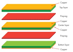
You start the board with copper bonded to fiberglass (Fig. 2). The top and bottom layers (typically industry-type FR4) have copper on what will become the outside of the PCB. The center layer is FR4 (green in Figure 2) with copper on both sides, comprising the two inside conductive layers. Prepreg (pink) is effectively the glue that holds the stack together. It can be just adhesive, or it can be a combination of FR4 fiberglass and thermal-setting adhesive. During the fabrication process, the stack will be compressed under heat and pressure to bond the layers together.
The order of construction can differ depending on many things. Our favorite reference resource, the handbook that most engineers call the “PC Bible,” is by Coombs.1 He details the PCB fabrication processes, outlining hundreds of variations and possibilities. Just when you are thoroughly intimidated, you get to the appendix.
The knowledge in the appendix is massive, a list of industry standards pertaining to everything PCB. It takes you from components including surface-mount, general, and passives to printed boards, materials, and design activities, then to component mounting and soldering, and through quality assessment, test methods, and repair. At this point we begin to appreciate and understand why we need our best board vendor to guide and advise us.
Still, mistakes do happen with boards, and it seems that they always occur just before a firm deadline. The four PCB examples below happened either before a bed-of-nails test of the bare board was available or after that test was eliminated to save time—always a bad practice that will punish us. Can you guess the errors that we found in each example?
Example 1: Over-etching
We received PCBs and assembled six boards. Oddly, the boards all had different issues. Normally when you fix one board that same fix applies to all the boards. But not this time, which was the key to understanding the problem.
We found that some of the errors were tiny shards of copper that shorted random things. Simultaneously, we were seeing a massive “passive” problem (at least we usually think that a PCB is passive) in the circuit’s performance. No circuit can function with dozens of random shorts. Because these shorts were random and different on each board, it was a troubleshooting nightmare. We sectioned the PCB and looked at it under a microscope. The board was over-etched.
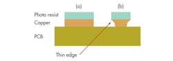
Figure 3a shows flat sides under photo resist. If the chemistry and temperature aren’t correct or if the board is in the etching solution too long, you’ll get etching “around the corner” that undercuts the copper (Fig. 3b). Long, thin shards can break off the top edge, stay connected on one end, and short to the adjacent traces.
Looking closely at our board, we saw two abrasive scratch-mark patterns at 90° angles. The vendor had used a polymer grinding wheel with an embedded abrasive. The vendor attempted to scrub off the shards by grinding the board in two passes on each side. Most of the shards were removed, but then the vendor solder-coated the board, which made the remaining shards solid random shorts. Adding solder mask hid the shorts and most grind marks.
Example 2: Orientation
We received a two-sided PCB with solder mask and top silkscreen and assembled a board by hand with through-hole parts. Nothing worked. We had a serious problem with the so-called passive PCB: all three power supplies were shorted in multiple places. Nothing made any sense. Not one circuit block out of dozens functioned at all. The technician tried, but finally had to call the engineer for help.
The technician managed to insert the parts in some strange ways. For example, the three leads of a transistor, which would normally form a triangle in the silkscreen outline, were distorted and twisted. Looking closely under the solder mask we realized that the silkscreen and the bottom side of the board were oriented properly, but the top component copper side of the board was a mirror image. The film used to make the topside image was upside down when the solder resist was exposed.
Example 3: Find Your Way
We received another four-layer board with similar issues. Again, many traces were connected to the wrong things, power supplies were shorted at multiple places, and nothing (no circuit block) worked. Usually when there is a board error, at least some of the circuits function. We had implemented a complete bed-of-nails test and were confused when it did not identify the issues.
Then we found out that the purchasing department skipped the bed-of-nails test to expedite board delivery. That test would have saved us days of effort. The wasted time was a costly error. We found that the board layers were assembled in the wrong order. Many blind vias were attached to the wrong layers. As a result, we added an edge code so we could inspect the boards (Fig. 4).
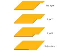
With the code implemented, we could quickly inspect the board layer order before we wasted time by populating the board with components.
The code extended to the edge of the PCB. Typically, boards are fabricated in larger panels made of many smaller PCBs to ease handling during fabrication. The individual boards are separated using a router, exposing the code on the board’s edge. A microscope lets us measure the copper spacing and see that it meets the board specification.
Example 4: The Right Thickness, But Not The Right Answer
We received a four-layer board. Most of it worked, but the striplines had huge ringing and reflections. Striplines are the equivalent of coaxial cables embedded into the PCB. A coax is a center conductor inside an insulating dielectric, surrounded with a circular ground shield. In addition to shielding the signal from external contamination, the coax and the stripline provide a known impedance signal path that, when terminated in its characteristic impedance, does not reflect energy. If the PCB is not constructed properly, the impedance change causes reflections and ringing that destroys analog signals and can even confuse digital signals.
Sectioning the board permitted us to measure the thickness of the various layers. We found that the PCB vendor had a shortage of some thicknesses of the board material. The vendor’s untrained employee tried to meet our delivery deadline and substituted extra prepreg layers from something in stock, making the total thickness correct. This might sound like a good “fix,” but it definitely was not so.
Look back at Figure 3. Let’s say that the center layer with copper on both sides was substituted with thinner material. The capacitance between those two layers will rise because the dielectric is thinner. To keep the layout and the final board the same total thickness, we can compensate by increasing the upper prepreg layer thickness. This will reduce the capacitance between the top copper and the nearest copper layer in the center. Note, however, that this also assumes the prepreg has the same dielectric constant in both cases, which may not be true. The change in capacitance then changes the PCB and stripline impedance, and our supposedly “passive” PCB is now ringing. You can say goodbye to signal integrity.
PCB Problems Cause Passive Failures
Clearly an unseen, taken-for-granted, whatever-you-want-to-call-it PCB exerts considerable influence on precision circuit performance. Moreover, we cannot take anything for granted nor assume that passive IC problems are unrelated to the PCB itself. Common IC performance problems and errors caused by a bad PCB include voltage drops and impedance in ground vias, planes or foils; leakage resistances and moisture absorption; and stray capacitance, with welcomed and dielectric absorption or soakage.
Voltage Drop
Voltage drop in ground vias, planes, or foils is a commonly overlooked issue. Adding to the complexity of the problem, voltage drops at both dc and high frequencies require different remedies. Recall Coombs’ Handbook,2 Chapter 10 for trace versus capacitance and crosstalk and Chapter 13 for voltage and ground copper thickness versus sheet resistance. For via impedance we look to Sayre:3
L = 5.08h [ln (4h/d) + 1]
where:
L = inductance of the via, nH
h = length of the via, inches
d = diameter of the via, inches
Using h = 0.0625 inch and d = 0.020 inch gives us a via inductance of 0.666 µH. How can we reduce this inductance? Place two, four, or more vias in parallel.
This is a good first-order approximation and is useful in thinking about signal integrity below a few hundred megahertz. For more details and consideration of the current return paths, we turn to Howard W. Johnson and his “Black Magic” series.4
Leakage Resistance
The leakage resistance5 of the PCB can disturb sensitive high-impedance circuits. The sources of leakage include improper selection of a laminate material, fingerprints, skin oils, human breath, residual fabrication chemicals, improperly cleaned solder flux, and surface moisture and humidity. If this is a problem for your circuit, consider surface and subsurface contamination and moisture absorption to be everywhere, on, in, or under the solder mask; on, in, or under conformal coatings; or on or in active or passive components.
When troubleshooting an existing PCB, remember an experienced engineer blowing on the board through a soda straw. The straw localizes the moisture to help identify the sensitive area. Thorough board cleaning with the proper solvents is important. For example, cleaning a water-soluble flux with a polar solvent can leave salts on the board. If deionized water is used to clean the boards, bake the boards to dry them.
Even now you may not be done. Even the cleanest board may still cause problems. A PCB with a very sensitive circuit such as an op amp with a high impedance input and high gain likely needs additional attention. It might be necessary to guard or surround the sensitive pins on all board layers with a driven low-impedance circuit matching the dc level of the guarded pins.6
Stray Capacitance
Capacitance is usually a problem when it is stray and unavoidable. It reduces bandwidth and slows high-speed signals. It is bad when dielectric absorption or soakage7 causes hooking, slew-rate errors, or undershoot/overshoot. However, capacitance is welcome when it is high-frequency power decoupling. We can specify a thinner than normal dielectric (even thin FR4) between the power and ground planes to increase the capacitance. Discrete capacitors smaller than 10 pF (self-resonant at ~2 GHz in surface mount) are easily compromised by trace and via inductance. Where the capacitance is distributed between power and ground planes, it has low series inductance and is repeatable if, yes, we have a “golden” PCB vendor.
Summary
Let’s think back to our opening magician’s mysterious box with hidden tricks. We expect certain norms and see what we expect. We simply cannot be that blind when it comes to the potential problems in a PCB. The manufacture and assembly of a board is far more complex than it appears to a casual examiner, and in that complexity lies the potential for PCB flaws and errors.
Those flaws and errors can introduce passive errors in ICs. We only examined voltage drop, leakage current, and stray capacitance, but the list of potential passive errors is indeed longer. Solving these passive problems inevitably means fixing the PCB, and each situation will demand its own solution. Finally, within this context we can all appreciate the contribution that a good reliable PCB vendor makes to our successful products.
This file type includes high resolution graphics and schematics when applicapable.
References
1. Coombs, Clyde F. Jr., Printed Circuits Handbook, sixth edition, McGraw Hill, 2008.
2. Coombs, op cit., Chapters 10 and 13.
3. Sayre, Cotter, Complete Wireless Design, McGraw-Hill, IBSN 978-0-07-154452-8, page 421 in first edition.
4. Johnson, Howard, High Speed Digital Design: A Handbook of Black Magic and High Speed Signal Propagation: Advanced Black Magic and Via Inductance at http://www.sigcon.com/Pubs/news/6_04.htm
5. Maxim Integrated tutorial 4429, “Murphy’s Law and the Risks of Designing ‘Off Data Sheet,’” Figure 3 and the following text, http://www.maximintegrated.com/app-notes/index.mvp/id/4429,
6. Maxim Integrated application note 3264, “Compact DWDM laser Temperature Control with the MAX8521,” Figure 2 and surrounding text, http://www.maximintegrated.com/app-notes/index.mvp/id/3264.
7. Laumeister, Bill, “Passives Aren’t Really So Passive: Part 1, Capacitors,” Electronic Design, June 4, 2013, http://electronicdesign.com/power/passive-components-aren-t-really-so-passive-part-1-capacitors
Bill Laumeister is an engineer in strategic applications with the Precision Control Group at Maxim Integrated. He works with customers who use DACs, digital potentiometers, and voltage references. He has more than 30 years of experience and holds several patents.
About the Author
Bill Laumeister
Bill Laumeister is an engineer in strategic applications at Maxim Integrated Products. He works with customers who use Maxim’s analog and digital integrated circuits. He has more than 30 years of experience and holds several patents.
Comment About the Article
To join the conversation, and become an exclusive member of Electronic Design, create an account today!

Leaders relevant to this article: